Dr. Cory FlynnThe Univ. of North Carolina, Ph.D. Chemistry, 2016 Wright State University, B.S. Chemistry, 2011 |

|
First Author
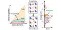
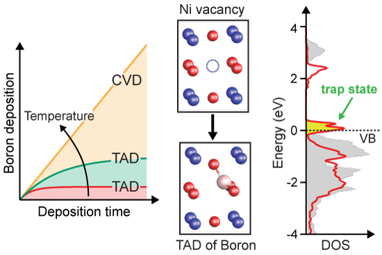
Localized trap states, which are deleterious to the performance of many solar-energy materials, often originate from the under-coordinated bonding associated with defects. Recently, the concept of targeted atomic deposition (TAD) was introduced as a process that permits the passivation of trap states using a vapor-phase precursor that selectively reacts with only the surface defect sites. Here, we demonstrate the passivation of nickel oxide (NiO) with the TAD process using diborane gas for selective, low-temperature deposition of boron (B) under continuous flow in a chemical vapor deposition (CVD) system. NiO is a ubiquitous cathode material used in dye-sensitized solar cells (DSSCs), organic photovoltaic devices, and organo-lead halide perovskite solar cells. The deposition of B at 100 °C is shown to follow first-order kinetics, exhibiting saturation at a B to Ni atomic ratio of ∼10%. Electrochemical measurements, combined with first-principles calculations, indicate that B passivates Ni vacancy defects by partially saturating the bonding of the oxygen atoms adjacent to the vacancy. p-Type DSSCs were fabricated using TAD-treated NiO and show a modest improvement in photovoltaic performance metrics. The results highlight the potential ubiquity of TAD passivation with a range of atomic precursors and vapor-phase processes.
ACS Applied Materials and Interfaces
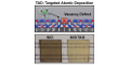
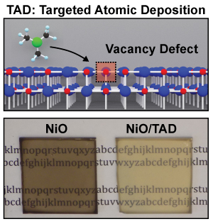
For nanomaterials, surface chemistry can dictate fundamental material properties, including charge-carrier lifetimes, doping levels, and electrical mobilities. In devices, surface defects are usually the key limiting factor for performance, particularly in solar-energy applications. Here, we develop a strategy to uniformly and selectively passivate defect sites in semiconductor nanomaterials using a vapor-phase process termed targeted atomic deposition (TAD). Because defects often consist of atomic vacancies and dangling bonds with heightened reactivity, we observe—for the widely used p-type cathode nickel oxide—that a volatile precursor such as trimethylaluminum can undergo a kinetically limited selective reaction with these sites. The TAD process eliminates all measurable defects in NiO, leading to a nearly 3-fold improvement in the performance of dye-sensitized solar cells. Our results suggest that TAD could be implemented with a range of vapor-phase precursors and be developed into a general strategy to passivate defects in zero-, one-, and two-dimensional nanomaterials.
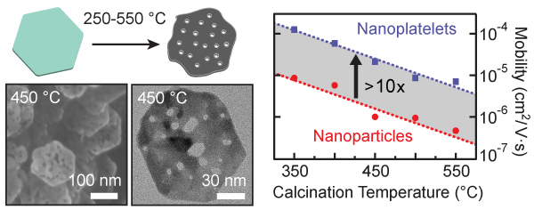
A p-type metal oxide with high surface area and good charge carrier mobility is of paramount importance for development of tandem solar fuel and dye-sensitized solar cell (DSSC) devices. Here, we report the synthesis, hierarchical morphology, electrical properties, and DSSC performance of mesoscale p-type NiO platelets. This material, which exhibits lateral dimensions of 100 nm but thicknesses less than 10 nm, can be controllably functionalized with a high-density array of vertical pores 4–6, 5–9, or 7–23 nm in diameter depending on exact synthetic conditions. Thin films of this porous but still quasi-two-dimensional material retain a high surface area and exhibit electrical mobilities more than 10-fold higher than comparable films of spherical particles with similar doping levels. These advantages lead to a modest, 20–30% improvement in the performance of DSSC devices under simulated 1-sun illumination. The capability to rationally control morphology provides a route for continued development of NiO as a high-efficiency material for tandem solar energy devices.
Contributing Author

Nano Letters
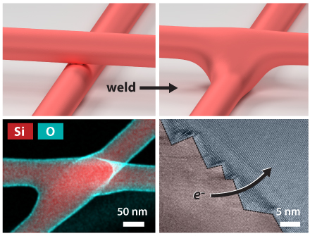
Semiconductor nanowires (NWs) have been demonstrated as a potential platform for a wide-range of technologies, yet a method to interconnect functionally encoded NWs has remained a challenge. Here, we report a simple capillarity-driven and self-limited welding process that forms mechanically robust and Ohmic inter-NW connections. The process occurs at the point-of-contact between two NWs at temperatures 400–600 °C below the bulk melting point of the semiconductor. It can be explained by capillarity-driven surface diffusion, inducing a localized geometrical rearrangement that reduces spatial curvature. The resulting weld comprises two fused NWs separated by a single, Ohmic grain boundary. We expect the welding mechanism to be generic for all types of NWs and to enable the development of complex interconnected networks for neuromorphic computation, battery and solar cell electrodes, and bioelectronic scaffolds.
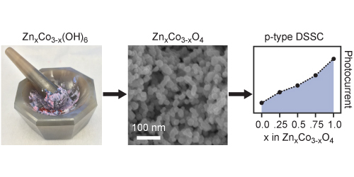
A solid-state mechanochemical synthesis of ZnxCo3−xO4 was developed with highly tunable Zn concentration. Photovoltaic performance was evaluated in dye-sensitized solar cells and tested with various Zn concentrations, exhibiting maximum performance with ZnCo2O4. Oxidative treatments led to a nearly three-fold increase in dye loading and a significant increase in short-circuit current density.
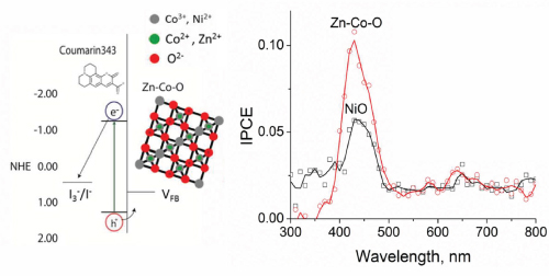
Tandem dye-sensitized solar cells that use nickel oxide as a hole-transport layer have limited performance due to the poor transport properties of NiO; alternative p-type oxides with the correct band alignment, good hole mobility, and stability in corrosive electrolyte must be identified. In this paper, we present our study on the ternary oxide material (zinc–cobalt–oxide spinel) as a hole conductor in a sensitized architecture. Zinc substitution for cobalt in cobalt(II,III) oxide results in good p-type conductivity and a spinel crystal structure. The flatband potential of Zn–Co–O thin films was determined to be around 0.7 V vs NHE (pH 5) and varies slightly depending on the conducting substrate. The films were used as the hole-transport layer in a dye-sensitized solar cell, and the hole-injection current was generated upon sensitization by coumarin-343. The cells exhibited an IQE of >90% and an open-circuit voltage of around 260 mV. The increase in photon-to-electron conversion efficiency of Zn–Co–O over NiO was due to an increased diffusion length, lower recombination, and better transport within the semiconductor-electrolyte device. Although the films were assembled here as liquid electrolyte dye-sensitized photovoltaic devices, they are also applicable to dye-sensitized photoelectrochemical cells for solar fuels.
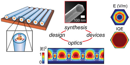
The silicon p–n junction is the most successful solar energy technology to date, yet it accounts for a marginal percentage of worldwide energy production. To change the status quo, a disruptive technological breakthrough is needed. In this Perspective, we discuss the potential for complex silicon nanowires to serve as a platform for next-generation photovoltaic devices. We review the synthesis, electrical characteristics, and optical properties of core/shell silicon nanowires that are subwavelength in diameter and contain radial p–n junctions. We highlight the unique features of these nanowires, such as optical antenna effects that concentrate light and intense built-in electric fields that enable ultrafast charge-carrier separation. We advocate a paradigm in which nanowires are arranged in periodic horizontal arrays to form ultrathin devices. Unlike conventional planar silicon, nanowire structures provide the flexibility to incorporate multiple semiconductor, dielectric, and metallic materials in a single system, providing the foundation for a disruptive, unconventional solar energy technology.
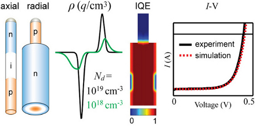
Semiconductor nanowires (NWs) are a developing platform for electronic and photonic technologies, and many demonstrated devices utilize a p-type/n-type (p–n) junction encoded along either the axial or radial directions of the wires. These miniaturized junctions enable a diverse range of functions, from sensors to solar cells, yet the physics of the devices has not been thoroughly evaluated. Here, we present finite-element modeling of axial and radial Si NW p–n junctions with total diameters of 240 nm and donor/acceptor doping levels ranging from 1016 to 1020 cm–3. We evaluate the photovoltaic performance of horizontally oriented NWs under 1 sun illumination and compare simulated current–voltage data to experimental measurements, permitting detailed analysis of NW performance, limitations, and prospect as a technology for solar energy conversion. Although high surface-to-volume ratios are cited as detrimental to NW performance, radial p–n junctions are surprisingly insensitive to surface recombination, with devices supporting open-circuit voltages (VOC) of 0.54 V and internal quantum efficiencies of 95% even with high surface recombination velocities (SRVs) of 105 cm/s. Axial devices, in which the depletion region is exposed to the surface, are far more sensitive to SRV, requiring substantially lower values of 103–104 cm/s to produce the same level of performance. For low values of the SRV (<100 cm/s), both axial and radial NWs can support VOC values of >0.70 V if the bulk minority carrier lifetime is 1 μs or greater. Experimental measurements on NWs grown by a vapor–liquid–solid mechanism yield VOC of 0.23 and 0.44 V for axial and radial NWs, respectively, and show that axial devices are limited by a SRV of 7 × 103 cm/s while radial devices are limited by a bulk lifetime of 3 ns. The simulations show that with further development the electrical characteristics of 200–300 nm Si NWs are sufficient to support power-conversion efficiencies of 15–25%. The analysis presented here can be generalized to other semiconductor homo- and heterojunctions, and we expect that insights from finite element modeling will serve as a powerful method to guide the design of advanced nanoscale structures.