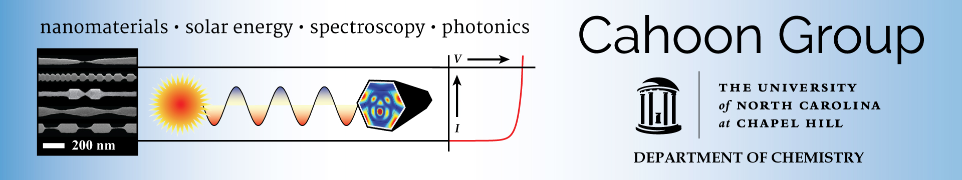
Research
We aim to understand and control the
physical properties of semiconductor nanomaterials through chemical synthesis. Our approach combines
material synthesis with physical measurements and in-house computational modeling to answer several
general questions, such as:
- What are the fundamental limits of size, composition, and morphology that can be chemically
encoded in a nanostructure?
- How does a material's morphology affect its interaction with light? Can absorption, scattering,
and waveguiding characteristics be entirely controlled through nanoscale morphology?
- How do charge carriers move and recombine in semiconductor nanostructures? How can the unique
characteristics of nanostructures, ranging from intense built-in fields to quantum confinement
effects, be used for new solar energy devices?
The materials we develop have applications
in solar and thermal energy, electronics, and photonics. By developing synthetic methods to control
nanomaterial composition, morphology, and doping, we create structures that can function as (1)
nanostructured solar cell devices, (2) a platform for hybrid semiconductor-molecular interfaces, or
(3) one-dimensional components of photonic, electronic, and thermal-energy devices. Nanomaterial
synthesis is coupled with optical and electronic experimental characterization using a range of
techniques from nanofabrication to micro-spectroscopy. In-house finite-element optical and device
modeling is used to interpret experimental measurements and design new materials, providing rapid
feedback between synthesis, measurement, and simulation. The approach is multidisciplinary,
interfacing chemistry, physics, materials science, and engineering.
Funding
 UNC College of Arts and Science
http://www.college.unc.edu
UNC College of Arts and Science
http://www.college.unc.edu
 Packard Foundation
http://www.packard.org/
Packard Foundation
http://www.packard.org/
 National Science Foundation (NSF)
http://www.nsf.gov
National Science Foundation (NSF)
http://www.nsf.gov
 Sloan Foundation
http://www.sloan.org
Sloan Foundation
http://www.sloan.org
 Research Corporation of Science Advancement
http://www.rescorp.org/
Research Corporation of Science Advancement
http://www.rescorp.org/
 Department of Energy (DOE)
CHASE
http://www.solarhub.unc.edu
Nanomaterial Synthesis
CVD System and Nanowire Growth
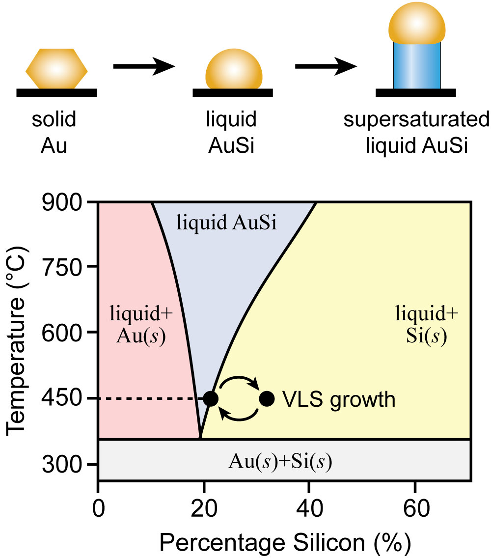
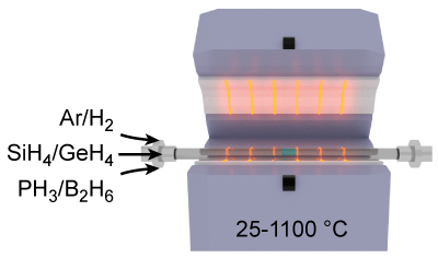
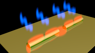
Semiconductor nanowires are synthesized through a home-built, hot-wall chemical vapor deposition
(CVD) system. This computer-controlled system enables detailed control of synthetic conditions
in order to grow group IV (Si, Ge) semiconductor nanowires. Our system allows for detailed
control of pressure, temperature, and flow rates of various precursor, doping, and carrier
gases. This precise, automated control allows for complex coaxial and radial dopant modulation,
core/shell morphologies, and even radically new nanowire geometries. For example, precise
modulation of phosphorus dopants along the nanowire axis in conjunction with wet chemical
etching can produce grating structures in a process termed ENGRAVE
(Encoded Nanowire GRowth and Appearance through VLS and
Etching).
Wet Chemical Synthesis
Our wet-chemical methods are optimized for nanoparticle synthesis. Standard equipment, including
round-bottom flasks, Erlenmeyers, filter flasks, heating mantles, condensers, stir plates, and
volumetric glassware, are regularly used to execute any necessary wet chemical synthesis. Our
capabilities include solvothermal synthesis in addition to sol-gel techniques. A large volume
multi-rotor centrifuge, Ika RV-10 rotovap with plastic coated glassware, several vacuum pumps, and
vacuum oven facilitate efficient and high yield collection of prepared samples. This equipment is
regularly used for synthesis of metal-oxide nanoparticles and nanoparticle pastes needed for
dye-sensitized solar cell devices. Additionally, our 12 position synchronous digital magnetic
stirrer with heating capabilities effectively maintains any sample requiring constant agitation. A
spin coater aids in the production of homogeneous thin films. A large volume box furnace can anneal
materials up to 1100 °C. Outside our own lab we have access to all the facilities and equipment
available in CHANL, Chapel Hill Analytical and Nanofabrication
Laboratory, and the EFRC fabrication laboratory.
Representative Publications
- "Encoding Abrupt and Uniform Dopant
Profiles in Vapor-Liquid-Solid Nanowires by Suppressing the Reservoir Effect of the Liquid
Catalyst" J.D. Christesen, C.W. Pinion, X. Zhang, J.R. McBride, and J.F. Cahoon. ACS
Nano, 8, 11790–11798 (2014).
- "Sensitized Zinc Cobalt Oxide Spinel
P-type Photoelectrodes" C.C. Mercado, A. Zakutayev, K. Zhu, C.J. Flynn, J.F. Cahoon, and
A.J. Nozik. J. Phys. Chem C., 118, 25340–25349 (2014).
- "Hierarchically-Structured NiO
Nanoplatelets as Mesoscale p-Type Photocathodes for Dye-Sensitized Solar Cells" C.J. Flynn,
E.E. Oh, S.M. McCullough, R.W. Call, C.L. Donley, R. Lopez, J.F. Cahoon. J. Phys. Chem
C., 118, 14177–14184 (2014).
- "Identifying
Crystallization and Incorporation Limited Regimes During Vapor-Liquid-Solid Growth of Si
Nanowires" C.W. Pinion, D.P. Nenon, J.D. Christesen, J.F. Cahoon. ACS Nano, 8,
6081-6088 (2014).
- "Synthetically
Encoding 10-nm Morphology in Silicon Nanowires" J.D. Christesen,* C.W. Pinion,* E.M.
Grumstrup, J.M. Papanikolas, J.F. Cahoon (*equal contribution). Nano Lett., 13,
6281-6286 (2013).
**Featured in
Nature Nanotechnology Research Highlights: "Nanofabrication: Engraving Nanowires"
Nanophotonics
Plasmonics
Scattering
Absorption


The synthesis of structures with sub-wavelength dimensions gives control over light-matter
interactions that are not possible with bulk materials. For example, these structures can absorb
light beyond their physical cross sections (antenna effect), create localized electric field
enhancements (as in SERS), and exhibit selective absorption resonances. The properties of these
structures depend strongly on their morphologies. The use of synthetic techniques to control the
growth of nanowires creates a wide range of optical properties among chemically similar structures.
Coupling these structures to gold and other metals can induce controllable surface plasmons, further
enhancing the manipulation of light.
Control of these photonic and plasmonic properties provides a path to advanced optical devices,
whether to enhance the efficiency of photovoltaic cells or to develop all-optical circuit
components.
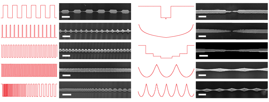
ENGRAVE (Encoded Nanowire GRowth and Appearance
through VLS and Etching)
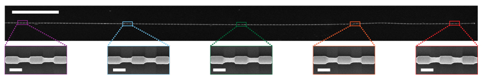
Until recently, the nanowire geometry had been limited to either smooth or faceted cylinders.
ENGRAVE, Encoded Nanowire Growth and Appearance through VLS and Etching, breaks these limitations
and allows full control of the nanowire geometry which opens up new avenues of uses for nanowires
from resistive memory to tunable SERS antennae. The geometry is controllable through the etch rate
of Silicon in KOH which is dependent on the doping level of Phosphorus in Silicon. The growth and
etch rates of the wire are used to calculate a dopant profile for the wire, the dopant profile is
then encoded using a precisely timed computer controlled system, and finally, a timed wet chemical
etch is used to reveal a complex structure. We have demonstrated this control of the ENGRAVE process
to produce periodic and non-periodic gratings, sinusoids, gaps, tapers, steps, and bow-ties as seen
in the figure below. Each SEM image has a red line which indicates the phosphine flow over the
length pictured in the SEM images.
Representative Publications
- "Doubling Absorption in Nanowire Solar
Cells with Dielectric Shell Optical Antennas" S.-K. Kim, X. Zhang, D.J Hill, K.-D. Song,
J.-S. Park, H.-G. Park, and J.F. Cahoon. Nano Lett., 15, 753–758 (2015).
- "Waveguide Scattering Microscopy for
Dark-Field Imaging and Spectroscopy of Photonic Nanostructures" D.J. Hill, C.W. Pinion, J.D.
Christesen, J.F. Cahoon. ACS Photonics (cover article), 1, 725–731 (2014).
- "Synthetically
Encoding 10-nm Morphology in Silicon Nanowires" J.D. Christesen,* C.W. Pinion,* E.M.
Grumstrup, J.M. Papanikolas, J.F. Cahoon (*equal contribution). Nano Lett., 13,
6281-6286 (2013).
**Featured in
Nature Nanotechnology Research Highlights: "Nanofabrication: Engraving Nanowires"
- "Horizontal
silicon nanowires with radial p-n junctions: A platform for unconventional solar cells" X.
Zhang,* C.W. Pinion,* J.D. Christesen, C.J. Flynn, T.A. Celano, J.F. Cahoon (*equal
contribution). J. Phys. Chem. Lett. (Invited Perspective), 4, 2002-2009 (2013).
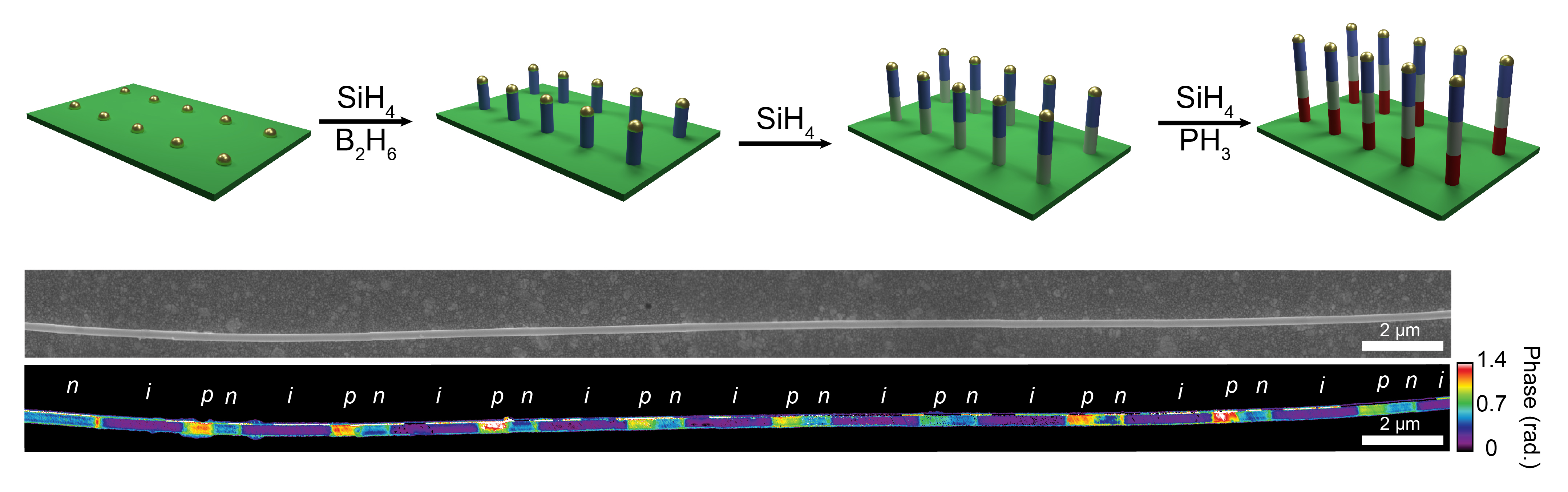
Multijunction Silicon Nanowires
Multijunction NW Growth
Nanowires are a promising platform on which to develop complex, nanostructured next-generation
photovoltaic (PV) devices. For silicon nanowires, PV devices can be synthesized by encoding n-type
and p-type dopants in the silicon during the wire growth. Through the VLS growth mechanism, we can
encode single nanowires with multiple p-i-n junctions. The dopant transition between each successive
unit is sufficiently abrupt to allow tunneling of charge carriers, and thus voltage summation across
an entire wire. This allows for tunable photovoltages of up to 10 V, well in excess of what is
needed to drive useful chemical reactions.
Device Fabrication
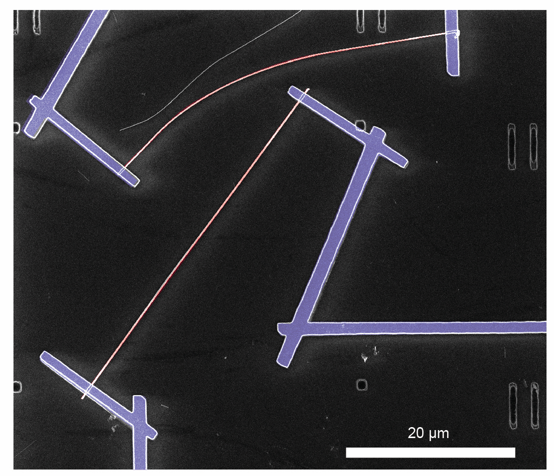
We have developed capability to synthesize prototype PV devices on length scales ranging from
millimeters to hundreds of nanometers. Prototype device fabrication is enabled by shared
electron-beam lithography and photolithography systems and high-quality metal evaporation
capabilities in the CHANL (Chapel Hill Analytical and
Nanofabrication Laboratory) user facility. Additional capabilities and equipment include
printed-circuit-board (PCB) fabrication, a wire bonder, a home-built probe station, measurement
system capable of femtoamp current readings, solar simulator, incident-photon-to-current-efficiency
(IPCE) optical system, and scanning optical microspectroscopy.
Particle Suspension Reactors
We aim to use our multijunction silicon nanowires as particulate photocatalysts for efficienct fuel
production. Our work focuses on aspects of wire design, catalyst design, and reactor engineering. We
look at the water splitting reaction using solid-state co-catalysts. We have developed a method to
spatioselectively deposit co-catalysts for specific reactions. We also look at using molecular
catalysts with our nanowires for CO2 reduction.
Measurement and Modeling
We use finite-element modeling as a core tool to design, predict, and understand both the optical and
electrical characteristics of the nanostructures, and quantitative comparison between experiment and
simulation is a key scientific approach in the group. Full-field wave-optics simulations can
generate accurate predictions of absorption and scattering in sub-wavelength structures. In
addition, device simulations can be used to simulate drift, diffusion, and recombination processes
in nanostructures, providing a detailed picture of internal fields and quantum efficiencies.
Furthermore, we have used these modeling tools to predict current-voltage characteristics that can
be directly compared with experiment. Finite-element simulations are performed entirely in-house
using the Comsol Multiphysics commercial software. The capability to perform these simulations in
house enables rapid feedback between design, synthesis, and measurement.
Representative Publications
- "Abrupt
degenerately-doped silicon nanowire tunnel junctions" C. Cordoba, T. Teitsworth, M. Yang,
J.F. Cahoon, K. Kavanagh. Nanotechnology, 31, 415708 (2020).
- "Interplay of Surface Recombination
and Diode Geometry for the Performance of Axial p-i-n Nanowire Solar Cells" D.J. Hill, T.S.
Teitsworth, E.T. Ritchie, J.M. Atkin, J.F. Cahoon. ACS Nano, 12, 10554–10563
(2018).
- "Mapping Free Carriers in
Multijunction Silicon Nanowires Using Infrared Near-Field Optical Microscopy" E.T. Ritchie,
D.J. Hill, T.M. Mastin, P.C. Deguzman, J.F. Cahoon, J.M. Atkin. Nano Letters, 17,
6591–6597 (2017).
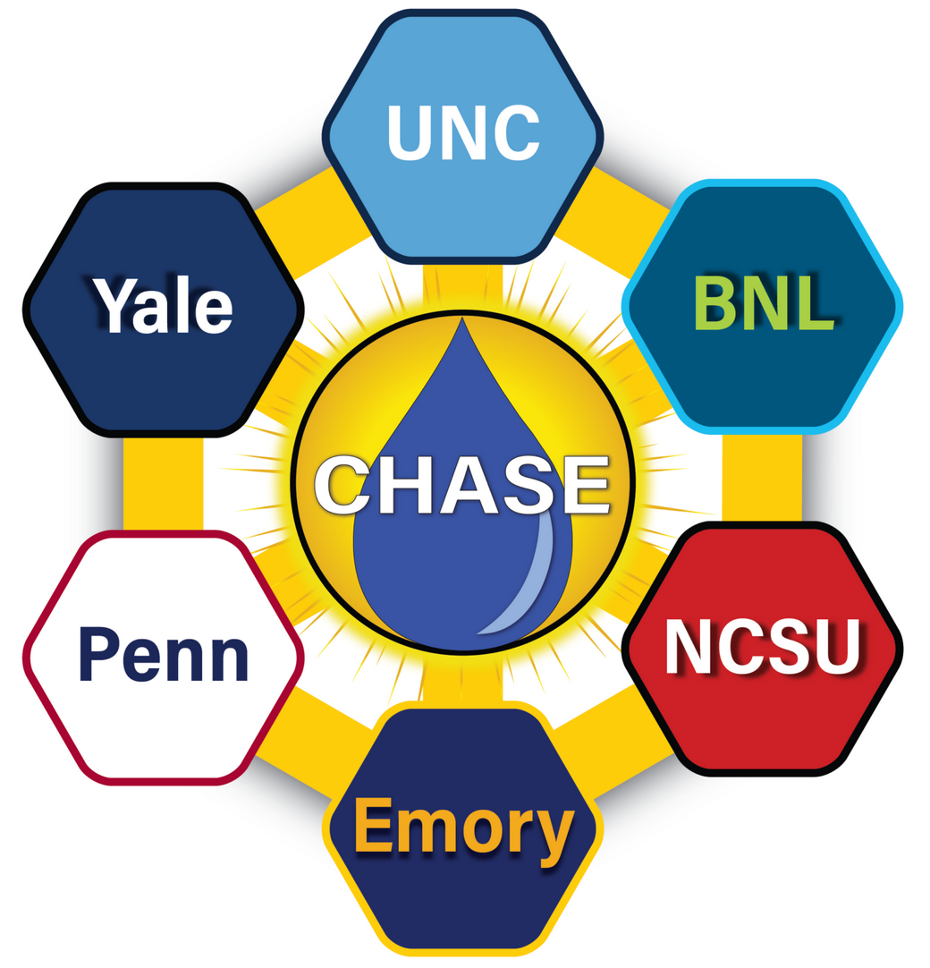
Solar Fuels
Hybrid Materials for Solar Fuels
The Center for Hybrid Approaches in Solar Energy to Liquid Fuels is a DOE
Energy Innovation Hub headquartered in the Chemistry Department at the University of North Carolina
at Chapel Hill.CHASE includes research partners at the University of North Carolina at Chapel Hill,
Yale University, Brookhaven National Laboratory, the University of Pennsylvania, North Carolina
State University, and Emory University and was initiated in 2020 by the U.S. Department of Energy
Office of Science, Office of Basic Energy Sciences. The CHASE mission is to develop
molecule/material hybrid photoelectrodes for cooperative sunlight-driven generation of liquid fuels
from carbon dioxide, nitrogen, and water. Pairing the light-absorbing properties of semiconductor
materials with the selective fuel-producing reactivity of molecular catalysts, CHASE will advance a
new paradigm of liquid solar fuels generation. This vast, mostly unexplored space at the
intersection between molecular catalysts and heterogeneous materials presents unique opportunities
for breakthroughs in photocatalyst durability and access to high-octane liquid fuels.
AI Accelerated Discovery of Solar Energy Materials
As shown by the images below, in a tandem DSPEC device light typically enters from the TiO2
photoanode, which is sensitized with a water oxidation chromophore-catalyst assembly that absorbs
light in the blue to red wavelength range. The lower energy (red to infrared) light is transmitted
through the water and a proton-exchange membrane to the photocathode, where light absorption with a
CO2 reduction chromophore-catalyst assembly occurs. The two halves of the device, photoanode and
photocathode, are connected in series and work together to efficiently generate solar fuels.
Representative Publications
- "Sensitized Zinc Cobalt Oxide Spinel
P-type Photoelectrodes" C.C. Mercado, A. Zakutayev, K. Zhu, C.J. Flynn, J.F. Cahoon, and
A.J. Nozik. J. Phys. Chem C., 118, 25340–25349 (2014).
- "Hierarchically-Structured NiO
Nanoplatelets as Mesoscale p-Type Photocathodes for Dye-Sensitized Solar Cells" C.J. Flynn,
E.E. Oh, S.M. McCullough, R.W. Call, C.L. Donley, R. Lopez, J.F. Cahoon. J. Phys. Chem
C., 118, 14177–14184 (2014).
Ultrafast Dynamics
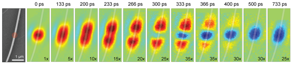
Pump-Probe Microscopy
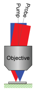
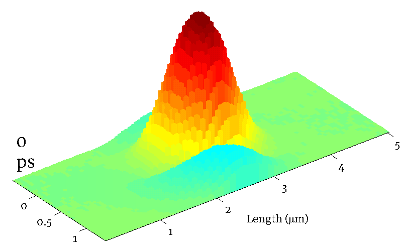
To understand the dynamics of charge carriers in semiconductor
nanostructures we probe the basic drift, diffusion, and recombination processes in single structures
using ultrafast microscopy. We have developed spatially-separated pump-probe (SSPP) microscopy, a
new technique which enables diffraction-limited imaging of charge carriers in space and time.
Shown to the right is an SSPP time-resolved movie of charge carriers in a single silicon nanowire.
At time zero, the image shows a diffraction-limited region of charge carriers. The charge carriers
diffuse and recombine on a picosecond time scale, causing broadening and decay of the signal
amplitude. The experiment provides direct information of the trap-state density and surface
recombination velocity in semiconductor nanostructures such as silicon nanowires.
Understanding Charge Carrier Recombination
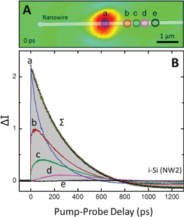
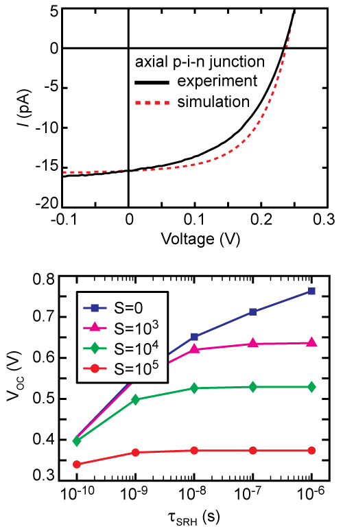
As shown by the images to the left, pump-probe microscopy provides a direct measurement of the charge
carrier lifetime at a specific spatial position in a nanowire. From this lifetime, we can determine
the surface recombination velocity (S) through the lifetime (τ) and diameter (d) due to the
relationship, S = d/4τ. This value for S can be directly compared to our I-V simulations on
photovoltaic nanowires with axial p-i-n junctions. As showing by the figures to the right, surface
recombination has a dramatic effect on photovoltaic device performance. Through direct comparison of
experiment and simulation, we were able to determine that the surface recombination velocity of an
axial p-i-n nanowire was 7 x 103 cm/s. This value is in good agreement with the value
obtained from the pump-probe measurements, S = 1.4 x 104 cm/s, for the same surface
treatement. The agreement of these measurements--one from devices and simulations and the other from
time-resolved microscopy--confirms the validity of both techniques and confirms that microscopy
provides direct information on the physical characteristics of nanowires that determine performance
in solar energy devices.
Representative Publications
- "Reversible Strain-Induced Electron-Hole
Recombination in Silicon Nanowires Observed with Femtosecond Pump-Probe Microscopy" E.M.
Grumstrup, M.M. Gabriel, C.W. Pinion, J.K. Parker, J.F. Cahoon, J.M. Papanikolas. Nano
Lett., 14, 6287–6292 (2014).
- "Imaging Charge Separation and Carrier
Recombination in Nanowire p-i-n Junctions Using Ultrafast Microscopy" M.M. Gabriel, E.M.
Grumstrup, J.R. Kirschbrown, C.W. Pinion, J.D. Christesen, D.F. Zigler, E.M. Cating, J.F.
Cahoon, J.M. Papanikolas. Nano Lett., 14, 3079-3087 (2014).
- "Ultrafast Carrier Dynamics in Individual Silicon
Nanowires: Characterization of Diameter-Dependent Carrier Lifetime and Surface Recombination
with Pump-Probe Microscopy" E.M. Grumstrup, M.M. Gabriel, E.M. Cating, C.W. Pinion, J.D.
Christesen, J.R. Kirschbrown, E.L. Vallorz, J.F. Cahoon, J.M. Papanikolas. J. Phys. Chem
C., 118, 8634-8640 (2014).
- "Ultrafast Carrier Dynamics of Silicon Nanowire
Ensembles: The Impact of Geometrical Heterogeneity on Charge Carrier Lifetime" E.M.
Grumstrup, E.M. Cating, M.M. Gabriel, C.W. Pinion, J.D. Christesen, J.R. Kirschbrown, E.L.
Vallorz, J.F. Cahoon, J.M. Papanikolas. J. Phys. Chem C., 118, 8626-8633 (2014).
- "Direct Imaging of
Free Carrier and Trap Carrier Motion in Silicon Nanowires by Spatially-Separated Femtosecond
Pump-Probe Microscopy" M.M. Gabriel,* J.R. Kirschbrown,* J.D. Christesen, C.W. Pinion, D.F.
Zigler, E.M. Grumstrup, B.P. Mehl, E. Cating, J.F. Cahoon, and J.M. Papanikolas (*equal
contribution). Nano Lett., 13, 1336-1340 (2013).
**Featured in
Nature Nanotechnology Research Highlights: "Charge Carriers Caught on Camera"
Electronics
Electron Ratchets
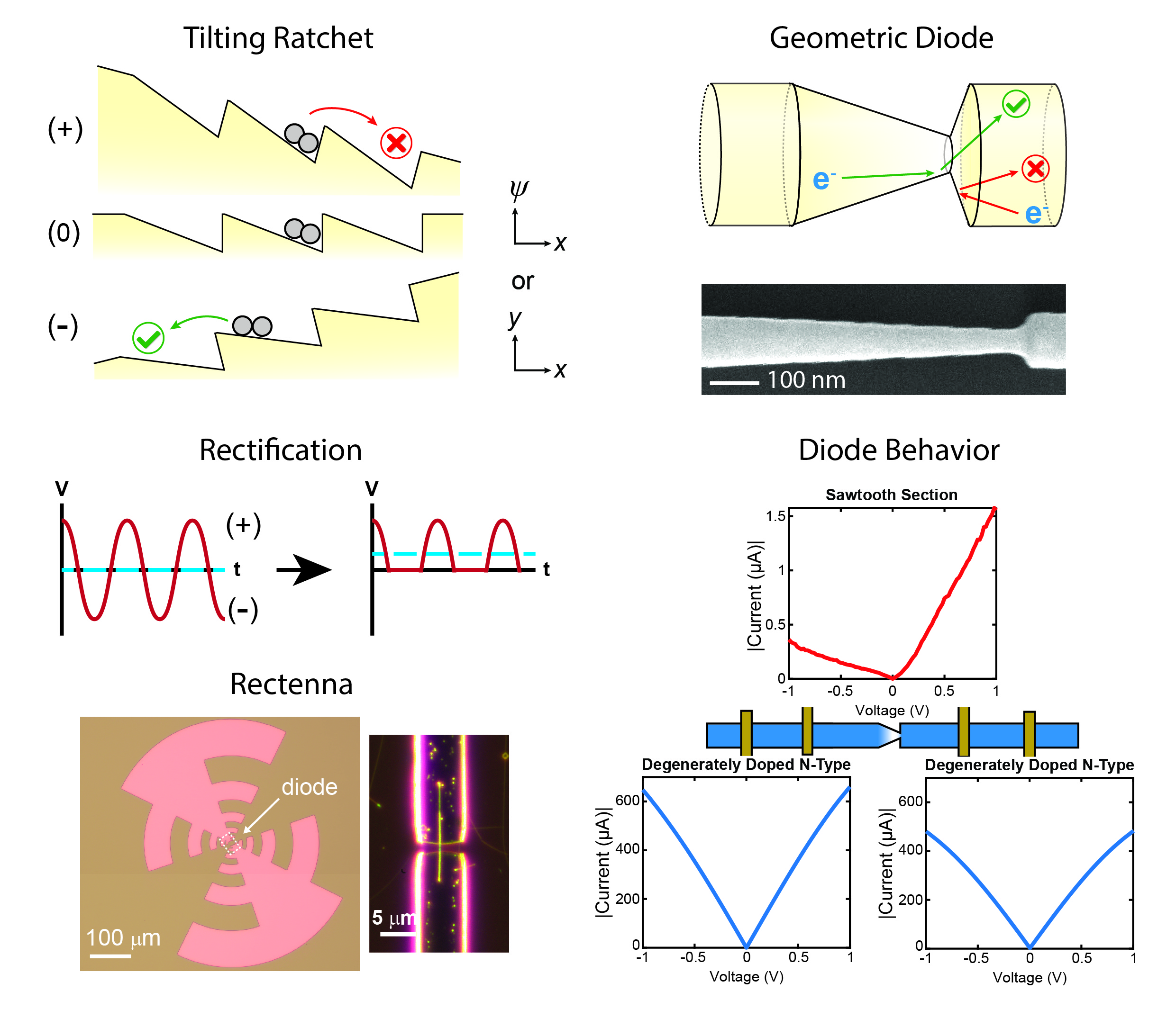
Electrical diodes for direct current and alternating current applications are typically
fabricated from semiconductor p-n junctions or metal-semiconductor Schottky junctions. Each
technology presents advantages and limitations in terms of the frequency of rectification,
reliability of fabrication, and integration on diverse or flexible substrates. We recently reported
an alternate strategy—two terminal geometric diodes—to produce zero-bias silicon diodes capable of
high-frequency rectification. The geometric diodes are spatially asymmetric, two-terminal majority
carrier devices operating via a ballistic mechanism, which causes the ratcheting of electrons and
generation of a DC bias upon application of an AC signal. The structures are grown from the
bottom-up by a vapor-liquid-solid growth process, producing single-crystalline nanowire structures
with precisely controlled asymmetric geometry and doping levels. As a result, we hypothesize that
with appropriate design the devices can rectify above 1 THz, and our current proof-of-concept
experimental results have demonstrated rectification through at least 40 GHz. We are currently
working toward understanding the design principles (synthesis conditions, surfaces, doping levels,
geometry, etc) that dictate geometric diode performance and evaluating THz operation by directly
coupling geometric diodes to antennas, creating rectennas that can be integrated on diverse
substrates for THz detection.
Representative Publications
- "Omega-Gate Silicon
Nanowire Geometric Diodes withReconfigurable Self-Switching Operation and THz
Rectification", K. L. White, G. V. Rogelberg, J. P. Custer Jr., J.F. Cahoon. Advanced
Electronic Materials (2023).
- "Influence of Geometry on
Quasi-Ballistic Behavior in Silicon Nanowire Geometric Diodes" K. L. White, M. A. Umanstev,
J. D. Low, J. P. Custer Jr., J. F. Cahoon. ACS Applied Nano Materials, 6, 5117–5126
(2023).
- "Ratcheting Quasi-ballistic
Electrons in Silicon Geometric Diodes at Room Temperature" J.P. Custer, J.D. Low, D.J. Hill,
T.S. Teitsworth, J.D. Christesen, C.J. McKinney, J.R. McBride, M.A. Brooke, S.C. Warren,
J.F. Cahoon. Science, 368, 177-180 (2020).
**Featured in
EuerkAlert! by AAAS
- "Synthetically
Encoding 10-nm Morphology in Silicon Nanowires" J.D. Christesen,* C.W. Pinion,* E.M.
Grumstrup, J.M. Papanikolas, J.F. Cahoon (*equal contribution). Nano Lett., 13,
6281-6286 (2013).
**Featured in
Nature Nanotechnology Research Highlights: "Nanofabrication: Engraving Nanowires"
Perovksites
Hybrid Perovskites
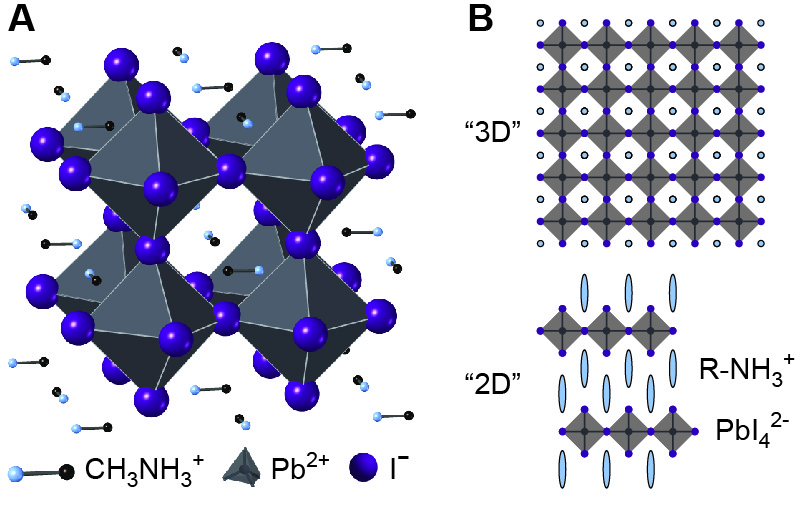
Hybrid perovskites (HPs), such as methylammonium lead halide (MAPbX3; MA = methylammonium,
CH3NH3+; X = Cl, Br, I), are an exciting class of semiconductor materials composed of organic and
inorganic constituents that have found unique functionality as thin films, macroscopic single
crystals, and colloidal nanocrystals for applications ranging from X-ray detectors to solar cells.
Depending on the size of the organic cation(s), the morphology of the material can be “3D”, “2D”, or
quasi-2D, composed of both larger and smaller organic cations with a mixture of 3D and 2D character.
The prominence of HP materials stems from exceptional electronic and physical properties—including
tunable bandgaps, defect tolerance, strong optical-absorption, and mechanically soft crystal
lattices—that make them suitable for varied optoelectronic and photovoltaic technologies. The
accessible solution-phase processing of HPs enabled the rise of an enormous volume of research and
rapid progress toward remarkably efficient photovoltaic devices. However, the vast majority of the
research focuses on solution-phase deposition, and vapor- and vacuum-based deposition techniques
that serve as workhorse methods in the semiconductor industry have been substantially less developed
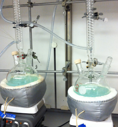
Reactor Design
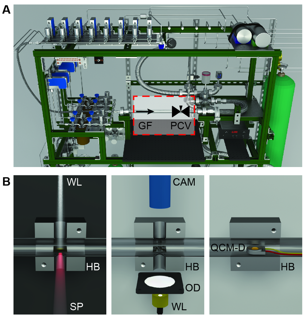
Metal organic chemical vapor deposition (MOCVD) emerged in the late 1960’s as a vital tool
to enable production of compound semiconductor and heterojunction devices, giving rise to
tremendously important technologies such as solid-state lighting and diode lasers. In light of this,
our group has designed a custom-built reactor to deposit HP thin films directly from the vapor phase
using separate lead, halide, and organic cation vapor sources, as well as integrating several in
situ characterization capabilities to monitor the growth process
MAPbX3 Fabrication
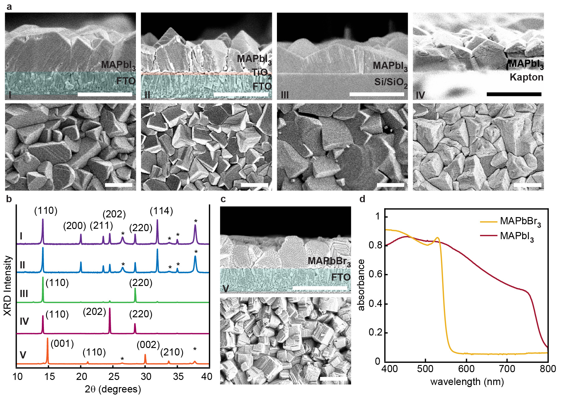
We have successfully deposited continuous thin films of MAPbX3 (X=I, Br) perovskites on
various substrates including transparent conductive oxides, silicon oxide, and flexible polymer
substrates (see figure). We’ve also used DFT molecular modeling to probe the mechanisms governing
these vapor-phase reactions. We expect further MOCVD process development will unlock unprecedented
compositional, crystallographic, and morphological control, enabling the precise design of material
properties and pursuit of new applications
Representative Publications
- "Metal Organic
Chemical Vapor Deposition of Hybrid Perovskites", A.C. Bryan, J.K. Meyers, L.Y. Serafin,
Z.A. Krajnak., R.J. Gentile, J.F. Cahoon. J. Am. Chem. Soc. (2025).
- " Identifying a “Raoult’s Law”
Relationship To Modulate the Stoichiometry of Hybrid Perovskite Films by
Amino-Deliquescence/Efflorescence in Mixed Amine Vapors", L.Y. Serafin, J.K. Meyers, A. C. Bryan, K.G. Broun, J. F. Cahoon. J. Phys. Chem. C
(2025).
- "Lithographically Patterning
Hybrid Perovskite Single Crystals by Surface-Engineered Amino-Deliquescence/Efflorescence"
J. K. Meyers, L. Y. Serafin, A. D. Orr, C. J. McKinney, J.F. Cahoon. ACS Photonics (2023).
- "Amino-Deliquescence and
Amino-Efflorescence of Methylammonium Lead Iodide" J.K. Meyers, L.Y. Serafin, A.D. Orr, J.F. Cahoon Chem. Mater. ,(2021).
We aim to understand and control the physical properties of semiconductor nanomaterials through chemical synthesis. Our approach combines material synthesis with physical measurements and in-house computational modeling to answer several general questions, such as:
- What are the fundamental limits of size, composition, and morphology that can be chemically encoded in a nanostructure?
- How does a material's morphology affect its interaction with light? Can absorption, scattering, and waveguiding characteristics be entirely controlled through nanoscale morphology?
- How do charge carriers move and recombine in semiconductor nanostructures? How can the unique characteristics of nanostructures, ranging from intense built-in fields to quantum confinement effects, be used for new solar energy devices?
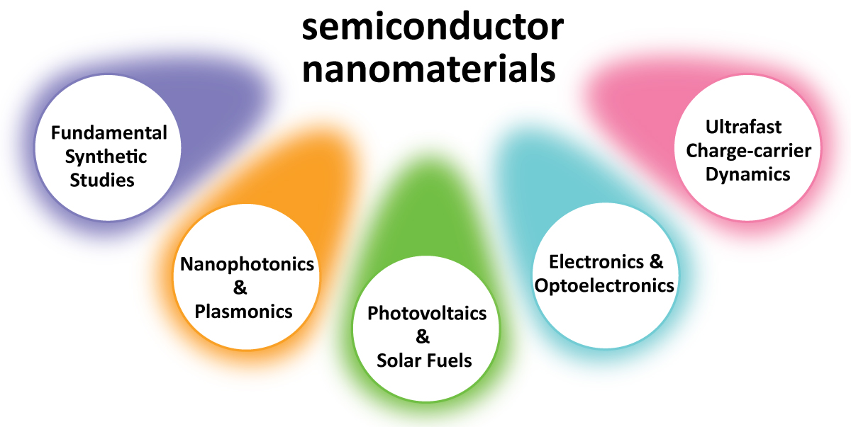
The materials we develop have applications in solar and thermal energy, electronics, and photonics. By developing synthetic methods to control nanomaterial composition, morphology, and doping, we create structures that can function as (1) nanostructured solar cell devices, (2) a platform for hybrid semiconductor-molecular interfaces, or (3) one-dimensional components of photonic, electronic, and thermal-energy devices. Nanomaterial synthesis is coupled with optical and electronic experimental characterization using a range of techniques from nanofabrication to micro-spectroscopy. In-house finite-element optical and device modeling is used to interpret experimental measurements and design new materials, providing rapid feedback between synthesis, measurement, and simulation. The approach is multidisciplinary, interfacing chemistry, physics, materials science, and engineering.
Funding
CHASE http://www.solarhub.unc.edu
Nanomaterial Synthesis
CVD System and Nanowire Growth
Semiconductor nanowires are synthesized through a home-built, hot-wall chemical vapor deposition (CVD) system. This computer-controlled system enables detailed control of synthetic conditions in order to grow group IV (Si, Ge) semiconductor nanowires. Our system allows for detailed control of pressure, temperature, and flow rates of various precursor, doping, and carrier gases. This precise, automated control allows for complex coaxial and radial dopant modulation, core/shell morphologies, and even radically new nanowire geometries. For example, precise modulation of phosphorus dopants along the nanowire axis in conjunction with wet chemical etching can produce grating structures in a process termed ENGRAVE (Encoded Nanowire GRowth and Appearance through VLS and Etching).
Wet Chemical Synthesis
Our wet-chemical methods are optimized for nanoparticle synthesis. Standard equipment, including round-bottom flasks, Erlenmeyers, filter flasks, heating mantles, condensers, stir plates, and volumetric glassware, are regularly used to execute any necessary wet chemical synthesis. Our capabilities include solvothermal synthesis in addition to sol-gel techniques. A large volume multi-rotor centrifuge, Ika RV-10 rotovap with plastic coated glassware, several vacuum pumps, and vacuum oven facilitate efficient and high yield collection of prepared samples. This equipment is regularly used for synthesis of metal-oxide nanoparticles and nanoparticle pastes needed for dye-sensitized solar cell devices. Additionally, our 12 position synchronous digital magnetic stirrer with heating capabilities effectively maintains any sample requiring constant agitation. A spin coater aids in the production of homogeneous thin films. A large volume box furnace can anneal materials up to 1100 °C. Outside our own lab we have access to all the facilities and equipment available in CHANL, Chapel Hill Analytical and Nanofabrication Laboratory, and the EFRC fabrication laboratory.
Representative Publications
- "Encoding Abrupt and Uniform Dopant Profiles in Vapor-Liquid-Solid Nanowires by Suppressing the Reservoir Effect of the Liquid Catalyst" J.D. Christesen, C.W. Pinion, X. Zhang, J.R. McBride, and J.F. Cahoon. ACS Nano, 8, 11790–11798 (2014).
- "Sensitized Zinc Cobalt Oxide Spinel P-type Photoelectrodes" C.C. Mercado, A. Zakutayev, K. Zhu, C.J. Flynn, J.F. Cahoon, and A.J. Nozik. J. Phys. Chem C., 118, 25340–25349 (2014).
- "Hierarchically-Structured NiO Nanoplatelets as Mesoscale p-Type Photocathodes for Dye-Sensitized Solar Cells" C.J. Flynn, E.E. Oh, S.M. McCullough, R.W. Call, C.L. Donley, R. Lopez, J.F. Cahoon. J. Phys. Chem C., 118, 14177–14184 (2014).
- "Identifying Crystallization and Incorporation Limited Regimes During Vapor-Liquid-Solid Growth of Si Nanowires" C.W. Pinion, D.P. Nenon, J.D. Christesen, J.F. Cahoon. ACS Nano, 8, 6081-6088 (2014).
- "Synthetically Encoding 10-nm Morphology in Silicon Nanowires" J.D. Christesen,* C.W. Pinion,* E.M. Grumstrup, J.M. Papanikolas, J.F. Cahoon (*equal contribution). Nano Lett., 13, 6281-6286 (2013). **Featured in Nature Nanotechnology Research Highlights: "Nanofabrication: Engraving Nanowires"
Nanophotonics
Plasmonics
Scattering
Absorption
The synthesis of structures with sub-wavelength dimensions gives control over light-matter interactions that are not possible with bulk materials. For example, these structures can absorb light beyond their physical cross sections (antenna effect), create localized electric field enhancements (as in SERS), and exhibit selective absorption resonances. The properties of these structures depend strongly on their morphologies. The use of synthetic techniques to control the growth of nanowires creates a wide range of optical properties among chemically similar structures. Coupling these structures to gold and other metals can induce controllable surface plasmons, further enhancing the manipulation of light.
Control of these photonic and plasmonic properties provides a path to advanced optical devices, whether to enhance the efficiency of photovoltaic cells or to develop all-optical circuit components.
ENGRAVE (Encoded Nanowire GRowth and Appearance through VLS and Etching)
Until recently, the nanowire geometry had been limited to either smooth or faceted cylinders. ENGRAVE, Encoded Nanowire Growth and Appearance through VLS and Etching, breaks these limitations and allows full control of the nanowire geometry which opens up new avenues of uses for nanowires from resistive memory to tunable SERS antennae. The geometry is controllable through the etch rate of Silicon in KOH which is dependent on the doping level of Phosphorus in Silicon. The growth and etch rates of the wire are used to calculate a dopant profile for the wire, the dopant profile is then encoded using a precisely timed computer controlled system, and finally, a timed wet chemical etch is used to reveal a complex structure. We have demonstrated this control of the ENGRAVE process to produce periodic and non-periodic gratings, sinusoids, gaps, tapers, steps, and bow-ties as seen in the figure below. Each SEM image has a red line which indicates the phosphine flow over the length pictured in the SEM images.
Representative Publications
- "Doubling Absorption in Nanowire Solar Cells with Dielectric Shell Optical Antennas" S.-K. Kim, X. Zhang, D.J Hill, K.-D. Song, J.-S. Park, H.-G. Park, and J.F. Cahoon. Nano Lett., 15, 753–758 (2015).
- "Waveguide Scattering Microscopy for Dark-Field Imaging and Spectroscopy of Photonic Nanostructures" D.J. Hill, C.W. Pinion, J.D. Christesen, J.F. Cahoon. ACS Photonics (cover article), 1, 725–731 (2014).
- "Synthetically Encoding 10-nm Morphology in Silicon Nanowires" J.D. Christesen,* C.W. Pinion,* E.M. Grumstrup, J.M. Papanikolas, J.F. Cahoon (*equal contribution). Nano Lett., 13, 6281-6286 (2013). **Featured in Nature Nanotechnology Research Highlights: "Nanofabrication: Engraving Nanowires"
- "Horizontal silicon nanowires with radial p-n junctions: A platform for unconventional solar cells" X. Zhang,* C.W. Pinion,* J.D. Christesen, C.J. Flynn, T.A. Celano, J.F. Cahoon (*equal contribution). J. Phys. Chem. Lett. (Invited Perspective), 4, 2002-2009 (2013).
Multijunction Silicon Nanowires
Multijunction NW Growth
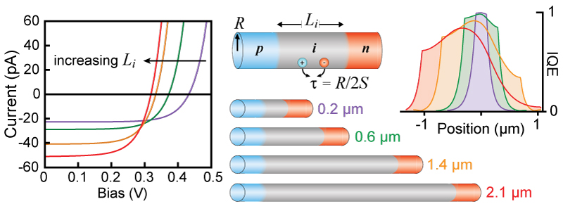
Nanowires are a promising platform on which to develop complex, nanostructured next-generation photovoltaic (PV) devices. For silicon nanowires, PV devices can be synthesized by encoding n-type and p-type dopants in the silicon during the wire growth. Through the VLS growth mechanism, we can encode single nanowires with multiple p-i-n junctions. The dopant transition between each successive unit is sufficiently abrupt to allow tunneling of charge carriers, and thus voltage summation across an entire wire. This allows for tunable photovoltages of up to 10 V, well in excess of what is needed to drive useful chemical reactions.
Device Fabrication
We have developed capability to synthesize prototype PV devices on length scales ranging from millimeters to hundreds of nanometers. Prototype device fabrication is enabled by shared electron-beam lithography and photolithography systems and high-quality metal evaporation capabilities in the CHANL (Chapel Hill Analytical and Nanofabrication Laboratory) user facility. Additional capabilities and equipment include printed-circuit-board (PCB) fabrication, a wire bonder, a home-built probe station, measurement system capable of femtoamp current readings, solar simulator, incident-photon-to-current-efficiency (IPCE) optical system, and scanning optical microspectroscopy.
Particle Suspension Reactors
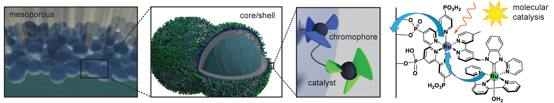
We aim to use our multijunction silicon nanowires as particulate photocatalysts for efficienct fuel production. Our work focuses on aspects of wire design, catalyst design, and reactor engineering. We look at the water splitting reaction using solid-state co-catalysts. We have developed a method to spatioselectively deposit co-catalysts for specific reactions. We also look at using molecular catalysts with our nanowires for CO2 reduction.
Measurement and Modeling
We use finite-element modeling as a core tool to design, predict, and understand both the optical and electrical characteristics of the nanostructures, and quantitative comparison between experiment and simulation is a key scientific approach in the group. Full-field wave-optics simulations can generate accurate predictions of absorption and scattering in sub-wavelength structures. In addition, device simulations can be used to simulate drift, diffusion, and recombination processes in nanostructures, providing a detailed picture of internal fields and quantum efficiencies. Furthermore, we have used these modeling tools to predict current-voltage characteristics that can be directly compared with experiment. Finite-element simulations are performed entirely in-house using the Comsol Multiphysics commercial software. The capability to perform these simulations in house enables rapid feedback between design, synthesis, and measurement.
Representative Publications
- "Abrupt degenerately-doped silicon nanowire tunnel junctions" C. Cordoba, T. Teitsworth, M. Yang, J.F. Cahoon, K. Kavanagh. Nanotechnology, 31, 415708 (2020).
- "Interplay of Surface Recombination and Diode Geometry for the Performance of Axial p-i-n Nanowire Solar Cells" D.J. Hill, T.S. Teitsworth, E.T. Ritchie, J.M. Atkin, J.F. Cahoon. ACS Nano, 12, 10554–10563 (2018).
- "Mapping Free Carriers in Multijunction Silicon Nanowires Using Infrared Near-Field Optical Microscopy" E.T. Ritchie, D.J. Hill, T.M. Mastin, P.C. Deguzman, J.F. Cahoon, J.M. Atkin. Nano Letters, 17, 6591–6597 (2017).
Solar Fuels
Hybrid Materials for Solar Fuels
The Center for Hybrid Approaches in Solar Energy to Liquid Fuels is a DOE
Energy Innovation Hub headquartered in the Chemistry Department at the University of North Carolina
at Chapel Hill.CHASE includes research partners at the University of North Carolina at Chapel Hill,
Yale University, Brookhaven National Laboratory, the University of Pennsylvania, North Carolina
State University, and Emory University and was initiated in 2020 by the U.S. Department of Energy
Office of Science, Office of Basic Energy Sciences. The CHASE mission is to develop
molecule/material hybrid photoelectrodes for cooperative sunlight-driven generation of liquid fuels
from carbon dioxide, nitrogen, and water. Pairing the light-absorbing properties of semiconductor
materials with the selective fuel-producing reactivity of molecular catalysts, CHASE will advance a
new paradigm of liquid solar fuels generation. This vast, mostly unexplored space at the
intersection between molecular catalysts and heterogeneous materials presents unique opportunities
for breakthroughs in photocatalyst durability and access to high-octane liquid fuels.
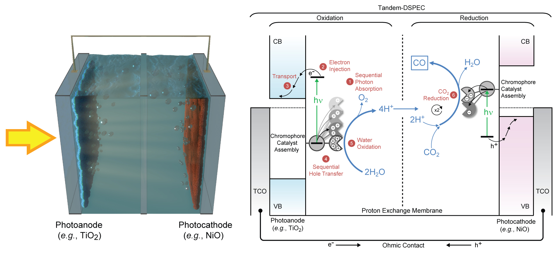
AI Accelerated Discovery of Solar Energy Materials
As shown by the images below, in a tandem DSPEC device light typically enters from the TiO2 photoanode, which is sensitized with a water oxidation chromophore-catalyst assembly that absorbs light in the blue to red wavelength range. The lower energy (red to infrared) light is transmitted through the water and a proton-exchange membrane to the photocathode, where light absorption with a CO2 reduction chromophore-catalyst assembly occurs. The two halves of the device, photoanode and photocathode, are connected in series and work together to efficiently generate solar fuels.
Representative Publications
- "Sensitized Zinc Cobalt Oxide Spinel P-type Photoelectrodes" C.C. Mercado, A. Zakutayev, K. Zhu, C.J. Flynn, J.F. Cahoon, and A.J. Nozik. J. Phys. Chem C., 118, 25340–25349 (2014).
- "Hierarchically-Structured NiO Nanoplatelets as Mesoscale p-Type Photocathodes for Dye-Sensitized Solar Cells" C.J. Flynn, E.E. Oh, S.M. McCullough, R.W. Call, C.L. Donley, R. Lopez, J.F. Cahoon. J. Phys. Chem C., 118, 14177–14184 (2014).
Ultrafast Dynamics
Pump-Probe Microscopy
To understand the dynamics of charge carriers in semiconductor nanostructures we probe the basic drift, diffusion, and recombination processes in single structures using ultrafast microscopy. We have developed spatially-separated pump-probe (SSPP) microscopy, a new technique which enables diffraction-limited imaging of charge carriers in space and time. Shown to the right is an SSPP time-resolved movie of charge carriers in a single silicon nanowire. At time zero, the image shows a diffraction-limited region of charge carriers. The charge carriers diffuse and recombine on a picosecond time scale, causing broadening and decay of the signal amplitude. The experiment provides direct information of the trap-state density and surface recombination velocity in semiconductor nanostructures such as silicon nanowires.
Understanding Charge Carrier Recombination
As shown by the images to the left, pump-probe microscopy provides a direct measurement of the charge carrier lifetime at a specific spatial position in a nanowire. From this lifetime, we can determine the surface recombination velocity (S) through the lifetime (τ) and diameter (d) due to the relationship, S = d/4τ. This value for S can be directly compared to our I-V simulations on photovoltaic nanowires with axial p-i-n junctions. As showing by the figures to the right, surface recombination has a dramatic effect on photovoltaic device performance. Through direct comparison of experiment and simulation, we were able to determine that the surface recombination velocity of an axial p-i-n nanowire was 7 x 103 cm/s. This value is in good agreement with the value obtained from the pump-probe measurements, S = 1.4 x 104 cm/s, for the same surface treatement. The agreement of these measurements--one from devices and simulations and the other from time-resolved microscopy--confirms the validity of both techniques and confirms that microscopy provides direct information on the physical characteristics of nanowires that determine performance in solar energy devices.
Representative Publications
- "Reversible Strain-Induced Electron-Hole Recombination in Silicon Nanowires Observed with Femtosecond Pump-Probe Microscopy" E.M. Grumstrup, M.M. Gabriel, C.W. Pinion, J.K. Parker, J.F. Cahoon, J.M. Papanikolas. Nano Lett., 14, 6287–6292 (2014).
- "Imaging Charge Separation and Carrier Recombination in Nanowire p-i-n Junctions Using Ultrafast Microscopy" M.M. Gabriel, E.M. Grumstrup, J.R. Kirschbrown, C.W. Pinion, J.D. Christesen, D.F. Zigler, E.M. Cating, J.F. Cahoon, J.M. Papanikolas. Nano Lett., 14, 3079-3087 (2014).
- "Ultrafast Carrier Dynamics in Individual Silicon Nanowires: Characterization of Diameter-Dependent Carrier Lifetime and Surface Recombination with Pump-Probe Microscopy" E.M. Grumstrup, M.M. Gabriel, E.M. Cating, C.W. Pinion, J.D. Christesen, J.R. Kirschbrown, E.L. Vallorz, J.F. Cahoon, J.M. Papanikolas. J. Phys. Chem C., 118, 8634-8640 (2014).
- "Ultrafast Carrier Dynamics of Silicon Nanowire Ensembles: The Impact of Geometrical Heterogeneity on Charge Carrier Lifetime" E.M. Grumstrup, E.M. Cating, M.M. Gabriel, C.W. Pinion, J.D. Christesen, J.R. Kirschbrown, E.L. Vallorz, J.F. Cahoon, J.M. Papanikolas. J. Phys. Chem C., 118, 8626-8633 (2014).
- "Direct Imaging of Free Carrier and Trap Carrier Motion in Silicon Nanowires by Spatially-Separated Femtosecond Pump-Probe Microscopy" M.M. Gabriel,* J.R. Kirschbrown,* J.D. Christesen, C.W. Pinion, D.F. Zigler, E.M. Grumstrup, B.P. Mehl, E. Cating, J.F. Cahoon, and J.M. Papanikolas (*equal contribution). Nano Lett., 13, 1336-1340 (2013). **Featured in Nature Nanotechnology Research Highlights: "Charge Carriers Caught on Camera"
Electronics
Electron Ratchets
Electrical diodes for direct current and alternating current applications are typically fabricated from semiconductor p-n junctions or metal-semiconductor Schottky junctions. Each technology presents advantages and limitations in terms of the frequency of rectification, reliability of fabrication, and integration on diverse or flexible substrates. We recently reported an alternate strategy—two terminal geometric diodes—to produce zero-bias silicon diodes capable of high-frequency rectification. The geometric diodes are spatially asymmetric, two-terminal majority carrier devices operating via a ballistic mechanism, which causes the ratcheting of electrons and generation of a DC bias upon application of an AC signal. The structures are grown from the bottom-up by a vapor-liquid-solid growth process, producing single-crystalline nanowire structures with precisely controlled asymmetric geometry and doping levels. As a result, we hypothesize that with appropriate design the devices can rectify above 1 THz, and our current proof-of-concept experimental results have demonstrated rectification through at least 40 GHz. We are currently working toward understanding the design principles (synthesis conditions, surfaces, doping levels, geometry, etc) that dictate geometric diode performance and evaluating THz operation by directly coupling geometric diodes to antennas, creating rectennas that can be integrated on diverse substrates for THz detection.
Representative Publications
- "Omega-Gate Silicon Nanowire Geometric Diodes withReconfigurable Self-Switching Operation and THz Rectification", K. L. White, G. V. Rogelberg, J. P. Custer Jr., J.F. Cahoon. Advanced Electronic Materials (2023).
- "Influence of Geometry on Quasi-Ballistic Behavior in Silicon Nanowire Geometric Diodes" K. L. White, M. A. Umanstev, J. D. Low, J. P. Custer Jr., J. F. Cahoon. ACS Applied Nano Materials, 6, 5117–5126 (2023).
- "Ratcheting Quasi-ballistic
Electrons in Silicon Geometric Diodes at Room Temperature" J.P. Custer, J.D. Low, D.J. Hill,
T.S. Teitsworth, J.D. Christesen, C.J. McKinney, J.R. McBride, M.A. Brooke, S.C. Warren,
J.F. Cahoon. Science, 368, 177-180 (2020).
**Featured in
EuerkAlert! by AAAS
- "Synthetically Encoding 10-nm Morphology in Silicon Nanowires" J.D. Christesen,* C.W. Pinion,* E.M. Grumstrup, J.M. Papanikolas, J.F. Cahoon (*equal contribution). Nano Lett., 13, 6281-6286 (2013). **Featured in Nature Nanotechnology Research Highlights: "Nanofabrication: Engraving Nanowires"
Perovksites
Hybrid Perovskites
Hybrid perovskites (HPs), such as methylammonium lead halide (MAPbX3; MA = methylammonium, CH3NH3+; X = Cl, Br, I), are an exciting class of semiconductor materials composed of organic and inorganic constituents that have found unique functionality as thin films, macroscopic single crystals, and colloidal nanocrystals for applications ranging from X-ray detectors to solar cells. Depending on the size of the organic cation(s), the morphology of the material can be “3D”, “2D”, or quasi-2D, composed of both larger and smaller organic cations with a mixture of 3D and 2D character. The prominence of HP materials stems from exceptional electronic and physical properties—including tunable bandgaps, defect tolerance, strong optical-absorption, and mechanically soft crystal lattices—that make them suitable for varied optoelectronic and photovoltaic technologies. The accessible solution-phase processing of HPs enabled the rise of an enormous volume of research and rapid progress toward remarkably efficient photovoltaic devices. However, the vast majority of the research focuses on solution-phase deposition, and vapor- and vacuum-based deposition techniques that serve as workhorse methods in the semiconductor industry have been substantially less developed
Reactor Design
Metal organic chemical vapor deposition (MOCVD) emerged in the late 1960’s as a vital tool to enable production of compound semiconductor and heterojunction devices, giving rise to tremendously important technologies such as solid-state lighting and diode lasers. In light of this, our group has designed a custom-built reactor to deposit HP thin films directly from the vapor phase using separate lead, halide, and organic cation vapor sources, as well as integrating several in situ characterization capabilities to monitor the growth process
MAPbX3 Fabrication
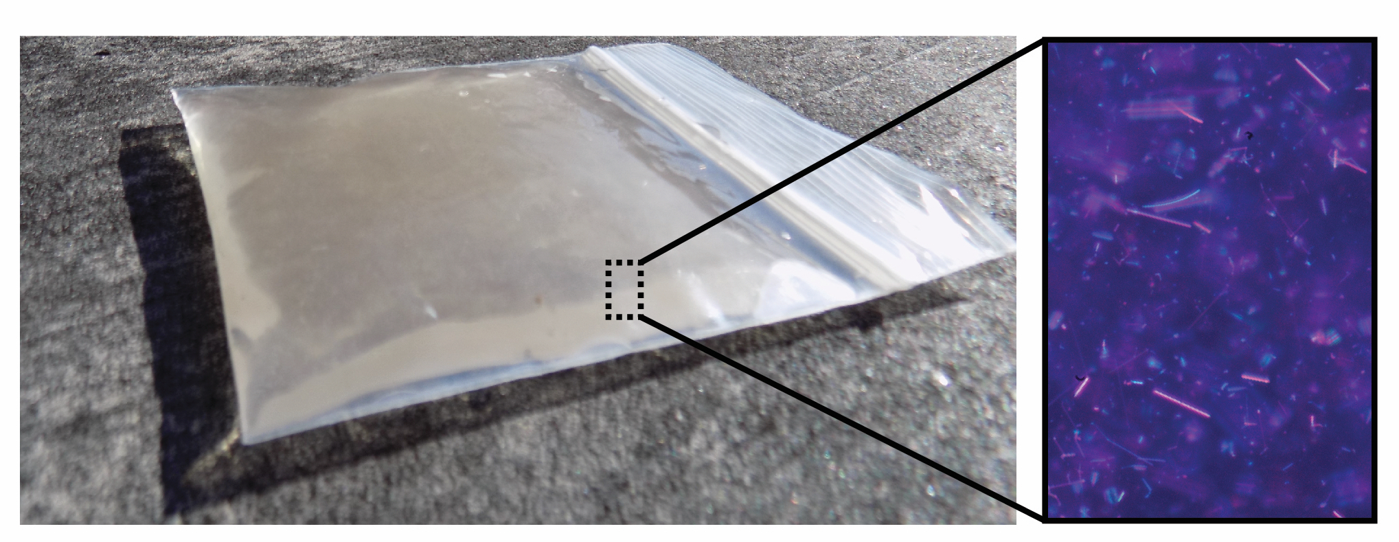
We have successfully deposited continuous thin films of MAPbX3 (X=I, Br) perovskites on various substrates including transparent conductive oxides, silicon oxide, and flexible polymer substrates (see figure). We’ve also used DFT molecular modeling to probe the mechanisms governing these vapor-phase reactions. We expect further MOCVD process development will unlock unprecedented compositional, crystallographic, and morphological control, enabling the precise design of material properties and pursuit of new applications
Representative Publications
- "Metal Organic Chemical Vapor Deposition of Hybrid Perovskites", A.C. Bryan, J.K. Meyers, L.Y. Serafin, Z.A. Krajnak., R.J. Gentile, J.F. Cahoon. J. Am. Chem. Soc. (2025).
- " Identifying a “Raoult’s Law” Relationship To Modulate the Stoichiometry of Hybrid Perovskite Films by Amino-Deliquescence/Efflorescence in Mixed Amine Vapors", L.Y. Serafin, J.K. Meyers, A. C. Bryan, K.G. Broun, J. F. Cahoon. J. Phys. Chem. C (2025).
- "Lithographically Patterning Hybrid Perovskite Single Crystals by Surface-Engineered Amino-Deliquescence/Efflorescence" J. K. Meyers, L. Y. Serafin, A. D. Orr, C. J. McKinney, J.F. Cahoon. ACS Photonics (2023).
- "Amino-Deliquescence and Amino-Efflorescence of Methylammonium Lead Iodide" J.K. Meyers, L.Y. Serafin, A.D. Orr, J.F. Cahoon Chem. Mater. ,(2021).