Kyoung-Ho KimKyoung-Ho Kim, Ph.D. Assistant Professor, Department of Physics Phone: +82-43-261-2271 PostDoc, UNC Chapel Hill, 2018 Ph.D in Physics, 2014 - The Korea University |

|
Contributing Author
Physical Review Letters
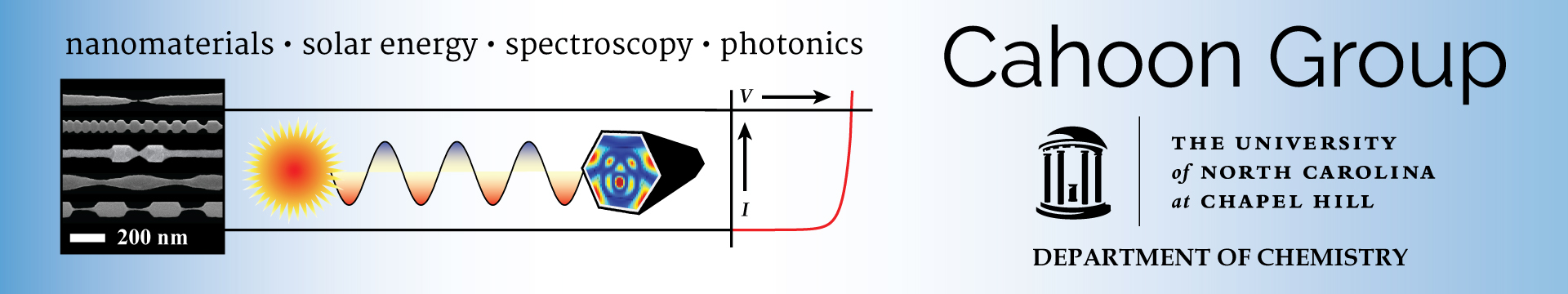
Perfect trapping of light in a subwavelength cavity is a key goal in nanophotonics. Perfect trapping has been realized with optical bound states in the continuum (BIC) in waveguide arrays and photonic crystals; yet the formal requirement of infinite periodicity has limited the experimental realization to structures with macroscopic planar dimensions. We characterize BICs in a silicon nanowire (NW) geometric superlattice (GSL) that exhibits one-dimensional periodicity in a compact cylindrical geometry with a subwavelength diameter. We analyze the scattering behavior of NW GSLs by formulating temporal coupled mode theory to include Lorenz-Mie scattering, and we show that GSL-based BICs can trap electromagnetic energy for an infinite lifetime and exist over a broad range of geometric parameters. Using synthesized NW GSLs tens of microns in length and with variable pitch, we demonstrate the progressive spectral shift and disappearance of Fano resonances in experimental single-NW extinction spectra as a manifestation of BIC GSL modes.
Nature Communications
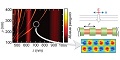
All-optical operation holds promise as the future of computing technology, and key components include miniaturized waveguides (WGs) and couplers that control narrow bandwidths. Nanowires (NWs) offer an ideal platform for nanoscale WGs, but their utility has been limited by the lack of a comprehensive coupling scheme with band selectivity. Here, we introduce a NW geometric superlattice (GSL) that allows narrow-band guiding in Si NWs through coupling of a Mie resonance with a bound-guided state (BGS). Periodic diameter modulation creates a Mie-BGS-coupled excitation that manifests as a scattering dark state with a pronounced scattering dip in the Mie resonance. The frequency of the coupled mode, tunable from the visible to near-infrared, is determined by the pitch of the GSL. Using a combined GSL-WG system, we demonstrate spectrally selective guiding and optical switching and sensing at telecommunication wavelengths, highlighting the potential to use NW GSLs for the design of on-chip optical components.
Nano Letters
We report the enhancement of light absorption in Si nanowire photovoltaic devices with one-dimensional dielectric or metallic gratings that are fabricated by a damage-free, precisely aligning, polymer-assisted transfer method. Incorporation of a Si3N4 grating with a Si nanowire effectively enhances the photocurrents for transverse-electric polarized light. The wavelength at which a maximum photocurrent is generated is readily tuned by adjusting the grating pitch. Moreover, the electrical properties of the nanowire devices are preserved before and after transferring the Si3N4 gratings onto Si nanowires, ensuring that the quality of pristine nanowires is not degraded during the transfer. Furthermore, we demonstrate Si nanowire photovoltaic devices with Ag gratings using the same transfer method. Measurements on the fabricated devices reveal approximately 27.1% enhancement in light absorption compared to that of the same devices without the Ag gratings without any degradation of electrical properties. We believe that our polymer-assisted transfer method is not limited to the fabrication of grating-incorporated nanowire photovoltaic devices but can also be generically applied for the implementation of complex nanoscale structures toward the development of multifunctional optoelectronic devices.