Tom CelanoPhD Chemistry, UNC Chapel Hill, 2017 North Carolina State University, B.S. Chemistry, 2011 |

|
First Author

Nano Letters
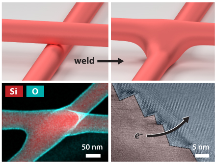
Semiconductor nanowires (NWs) have been demonstrated as a potential platform for a wide-range of technologies, yet a method to interconnect functionally encoded NWs has remained a challenge. Here, we report a simple capillarity-driven and self-limited welding process that forms mechanically robust and Ohmic inter-NW connections. The process occurs at the point-of-contact between two NWs at temperatures 400–600 °C below the bulk melting point of the semiconductor. It can be explained by capillarity-driven surface diffusion, inducing a localized geometrical rearrangement that reduces spatial curvature. The resulting weld comprises two fused NWs separated by a single, Ohmic grain boundary. We expect the welding mechanism to be generic for all types of NWs and to enable the development of complex interconnected networks for neuromorphic computation, battery and solar cell electrodes, and bioelectronic scaffolds.
Contributing Author
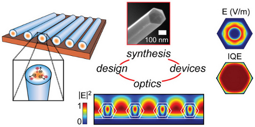
The silicon p–n junction is the most successful solar energy technology to date, yet it accounts for a marginal percentage of worldwide energy production. To change the status quo, a disruptive technological breakthrough is needed. In this Perspective, we discuss the potential for complex silicon nanowires to serve as a platform for next-generation photovoltaic devices. We review the synthesis, electrical characteristics, and optical properties of core/shell silicon nanowires that are subwavelength in diameter and contain radial p–n junctions. We highlight the unique features of these nanowires, such as optical antenna effects that concentrate light and intense built-in electric fields that enable ultrafast charge-carrier separation. We advocate a paradigm in which nanowires are arranged in periodic horizontal arrays to form ultrathin devices. Unlike conventional planar silicon, nanowire structures provide the flexibility to incorporate multiple semiconductor, dielectric, and metallic materials in a single system, providing the foundation for a disruptive, unconventional solar energy technology.
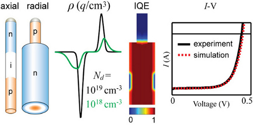
Semiconductor nanowires (NWs) are a developing platform for electronic and photonic technologies, and many demonstrated devices utilize a p-type/n-type (p–n) junction encoded along either the axial or radial directions of the wires. These miniaturized junctions enable a diverse range of functions, from sensors to solar cells, yet the physics of the devices has not been thoroughly evaluated. Here, we present finite-element modeling of axial and radial Si NW p–n junctions with total diameters of 240 nm and donor/acceptor doping levels ranging from 1016 to 1020 cm–3. We evaluate the photovoltaic performance of horizontally oriented NWs under 1 sun illumination and compare simulated current–voltage data to experimental measurements, permitting detailed analysis of NW performance, limitations, and prospect as a technology for solar energy conversion. Although high surface-to-volume ratios are cited as detrimental to NW performance, radial p–n junctions are surprisingly insensitive to surface recombination, with devices supporting open-circuit voltages (VOC) of 0.54 V and internal quantum efficiencies of 95% even with high surface recombination velocities (SRVs) of 105 cm/s. Axial devices, in which the depletion region is exposed to the surface, are far more sensitive to SRV, requiring substantially lower values of 103–104 cm/s to produce the same level of performance. For low values of the SRV (<100 cm/s), both axial and radial NWs can support VOC values of >0.70 V if the bulk minority carrier lifetime is 1 μs or greater. Experimental measurements on NWs grown by a vapor–liquid–solid mechanism yield VOC of 0.23 and 0.44 V for axial and radial NWs, respectively, and show that axial devices are limited by a SRV of 7 × 103 cm/s while radial devices are limited by a bulk lifetime of 3 ns. The simulations show that with further development the electrical characteristics of 200–300 nm Si NWs are sufficient to support power-conversion efficiencies of 15–25%. The analysis presented here can be generalized to other semiconductor homo- and heterojunctions, and we expect that insights from finite element modeling will serve as a powerful method to guide the design of advanced nanoscale structures.