Seokhyoung KimCaudill 008 (919) 843-6852 Education: B.S. Chemistry, 2012, Pohang University of Science and Technology M.S. Polymer Science and Engineering, 2013, University of Massachusetts, Amherst |

|
First Author
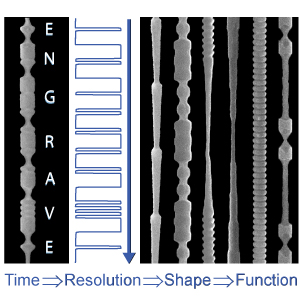
Comprehensive control of light–matter interactions at the nanoscale is increasingly important for the development of miniaturized light-based technologies that have applications ranging from information processing to sensing. Control of light in nanoscale structures—the realm of nanophotonics—requires precise control of geometry on a few-nanometer length scale. From a chemist’s perspective, bottom-up growth of nanoscale materials from chemical precursors offers a unique opportunity to design structures atom-by-atom that exhibit desired properties. In this Account, we describe our efforts to create chemically and morphologically precise Si nanowires (NWs) with designed nanophotonic properties using a vapor–liquid–solid (VLS) growth process. A synthetic technique termed “Encoded Nanowire Growth and Appearance through VLS and Etching” (ENGRAVE) combines optimized VLS growth, dopant modulation, and dopant-dependent wet-chemical etching to produce NWs with precisely designed diameter modulations, yielding lithographic-like morphological control that can vary from sinusoids to fractals. The ENGRAVE NWs thus provide a versatile playground for coupling, trapping, and directing light in a nanoscale geometry...
Physical Review Letters
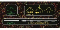
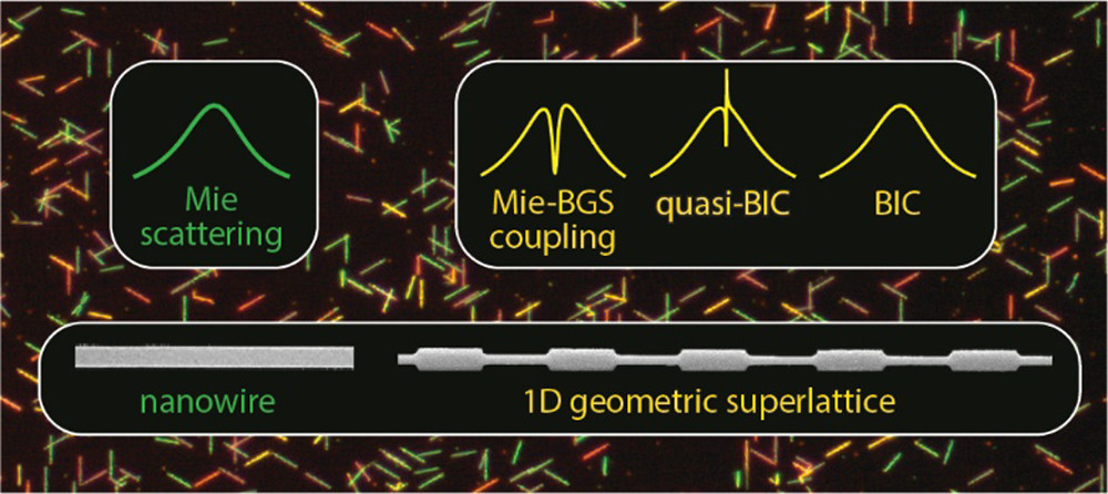
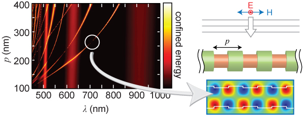
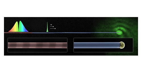
Perfect trapping of light in a subwavelength cavity is a key goal in nanophotonics. Perfect trapping has been realized with optical bound states in the continuum (BIC) in waveguide arrays and photonic crystals; yet the formal requirement of infinite periodicity has limited the experimental realization to structures with macroscopic planar dimensions. We characterize BICs in a silicon nanowire (NW) geometric superlattice (GSL) that exhibits one-dimensional periodicity in a compact cylindrical geometry with a subwavelength diameter. We analyze the scattering behavior of NW GSLs by formulating temporal coupled mode theory to include Lorenz-Mie scattering, and we show that GSL-based BICs can trap electromagnetic energy for an infinite lifetime and exist over a broad range of geometric parameters. Using synthesized NW GSLs tens of microns in length and with variable pitch, we demonstrate the progressive spectral shift and disappearance of Fano resonances in experimental single-NW extinction spectra as a manifestation of BIC GSL modes.
Nature Communications
All-optical operation holds promise as the future of computing technology, and key components include miniaturized waveguides (WGs) and couplers that control narrow bandwidths. Nanowires (NWs) offer an ideal platform for nanoscale WGs, but their utility has been limited by the lack of a comprehensive coupling scheme with band selectivity. Here, we introduce a NW geometric superlattice (GSL) that allows narrow-band guiding in Si NWs through coupling of a Mie resonance with a bound-guided state (BGS). Periodic diameter modulation creates a Mie-BGS-coupled excitation that manifests as a scattering dark state with a pronounced scattering dip in the Mie resonance. The frequency of the coupled mode, tunable from the visible to near-infrared, is determined by the pitch of the GSL. Using a combined GSL-WG system, we demonstrate spectrally selective guiding and optical switching and sensing at telecommunication wavelengths, highlighting the potential to use NW GSLs for the design of on-chip optical components.
ACS Nano
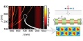
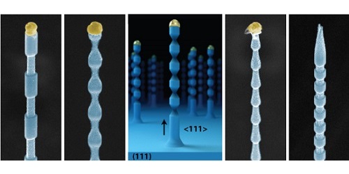
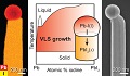
Vertically aligned semiconductor nanowires (NWs) have many potential applications for NW-based technologies, ranging from solar cells to intracellular sensors. Aligned NWs can be fabricated by top-down etching of planar wafers or synthesized from the bottom up using the vapor–liquid–solid (VLS) mechanism to induce epitaxial growth on lattice-matched substrates. The VLS process permits the modulation of dopants along the NW growth axis, which if combined with dopant-dependent wet-chemical etching, can be used to encode precise morphology. However, the synthesis of vertical and linear NWs with complex morphology is nontrivial, requiring control over multiple interdependent aspects of the VLS process. Here, we demonstrate sub-10 nm morphology in ⟨111⟩ epitaxial silicon (Si) NWs grown by the VLS mechanism on (111) Si substrates with gold (Au) catalysts. Using silane (SiH4), phosphine (PH3), and hydrochloric acid (HCl) precursor gases at 480 °C, precise morphology is encoded through abrupt phosphorus (P) dopant transitions, which are found to be less than 5 nm in width. The results highlight three mechanistic attributes of the process. First, NW growth in the ⟨111⟩ direction is found to be unstable at high SiH4 partial pressures and growth rates unless using HCl, which stabilizes NW growth through chlorination of the NW sidewall. Second, aggregated Au deposited on the NW surface by the VLS catalyst is found to be immobile on the chlorinated surface and to impede selective wet-chemical etching by potassium hydroxide (KOH) solution, preventing the design of precise morphology. Third, the aggregation of Au is found to be strongly dependent on the SiH4 partial pressure and NW growth rate, and values exceeding ∼100 mTorr and ∼150 nm/min, respectively, are required to minimize Au and thereby enable selective wet-chemical etching. Under optimized growth conditions, we find that abrupt, complex, and arbitrary dopant profiles and morphologies can be encoded in vertical Si NWs, and we expect that a variety of electronic and photonic applications can be realized with these designed nanostructures.
Contributing Author
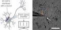
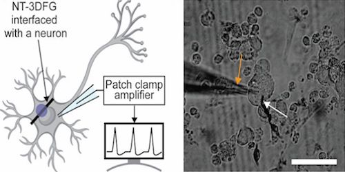
The ability to modulate cellular electrophysiology is fundamental to the investigation of development, function, and disease. Currently, there is a need for remote, nongenetic, light-induced control of cellular activity in two-dimensional (2D) and three-dimensional (3D) platforms. Here, we report a breakthrough hybrid nanomaterial for remote, nongenetic, photothermal stimulation of 2D and 3D neural cellular systems. We combine one-dimensional (1D) nanowires (NWs) and 2D graphene flakes grown out-of-plane for highly controlled photothermal stimulation at subcellular precision without the need for genetic modification, with laser energies lower than a hundred nanojoules, one to two orders of magnitude lower than Au-, C-, and Si-based nanomaterials. Photothermal stimulation using NW-templated 3D fuzzy graphene (NT-3DFG) is flexible due to its broadband absorption and does not generate cellular stress. Therefore, it serves as a powerful toolset for studies of cell signaling within and between tissues and can enable therapeutic interventions.
Nano Letters
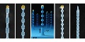
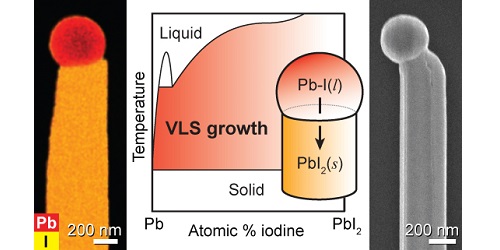
Lead halide perovskites (LHPs) have shown remarkable promise for use in photovoltaics, photodetectors, light-emitting diodes, and lasers. Although solution-processed polycrystalline films are the most widely studied morphology, LHP nanowires (NWs) grown by vapor-phase processes offer the potential for precise control over crystallinity, phase, composition, and morphology. Here, we report the first demonstration of self-catalyzed vapor–liquid–solid (VLS) growth of lead halide (PbX2; X = Cl, Br, or I) NWs and conversion to LHP. We present a kinetic model of the PbX2 NW growth process in which a liquid Pb catalyst is supersaturated with halogen X through vapor-phase incorporation of both Pb and X, inducing growth of a NW. For PbI2, we show that the NWs are single-crystalline, oriented in the ⟨1̅21̅0⟩ direction, and composed of a stoichiometric PbI2 shaft with a spherical Pb tip. Low-temperature vapor-phase intercalation of methylammonium iodide converts the NWs to methylammonium lead iodide (MAPbI3) perovskite while maintaining the NW morphology. Single-NW experiments comparing measured extinction spectra with optical simulations show that the NWs exhibit a strong optical antenna effect, leading to substantially enhanced scattering efficiencies and to absorption efficiencies that can be more than twice that of thin films of the same thickness. Further development of the self-catalyzed VLS mechanism for lead halide and perovskite NWs should enable the rational design of nanostructures for various optoelectronic technologies, including potentially unique applications such as hot-carrier solar cells.
ACS Applied Materials and Interfaces
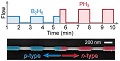
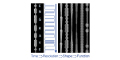
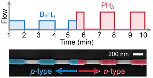
Although silicon (Si) nanowires (NWs) grown by a vapor–liquid–solid (VLS) mechanism have been demonstrated for a range of photonic, electronic, and solar-energy applications, continued progress with these NW-based technologies requires increasingly precise compositional and morphological control of the growth process. However, VLS growth typically encounters problems such as nonselective deposition on sidewalls, inadvertent kinking, unintentional or inhomogeneous doping, and catalyst-induced compositional gradients. Here, we overcome several of these difficulties and report the synthesis of uniform, linear, and degenerately doped Si NW superlattices with abrupt transitions between p-type, intrinsic, and n-type segments. The synthesis of these structures is enabled by in situ chlorination of the NW surface with hydrochloric acid (HCl) at temperatures ranging from 500 to 700 °C, yielding uniform NWs with minimal nonselective growth. Surprisingly, we find the boron (B) doping level in p-type segments to be at least 1 order of magnitude above the solid solubility limit, an effect that we attribute to a high incorporation of B in the liquid catalyst and kinetic trapping of B during crystallization at the liquid–solid interface to yield a highly nonequilibrium concentration. For growth at 510 °C, four-point-probe measurements yield active doping levels of at least 4.5 × 10^19 cm–3, which is comparable to the phosphorus (P) doping level of n-type segments. Because the B and P dopants are in sufficiently high concentrations for the Si to be degenerately doped, both segments inhibit the etching of Si in aqueous potassium hydroxide (KOH) solution. Moreover, we find that the dopant transitions are abrupt, facilitating nanoscale morphological control in both B- and P-doped segments through selective KOH etching of the NW with a spatial resolution of ∼10 nm. The results presented herein enable the growth of complex, degenerately doped p–n junction nanostructures that can be explored for a variety of advanced applications, such as Esaki diodes, multijunction solar cells, and tunneling field-effect transistors.
ACS Journal of Physical Chemistry Letters
The patterning of semiconductors with nanometer-scale precision is a cornerstone of modern technology. Top-down methods, ranging from photolithography to focused-ion beam milling, are typically used to fabricate complex nanostructures. In this Perspective, we discuss an alternative bottom-up method to encode similar high-resolution morphology in semiconductor nanowires (NWs). This process, termed ENGRAVE for “Encoded Nanowire GRowth and Appearance through VLS and Etching”, combines fast modulation of nanowire composition during vapor–liquid–solid (VLS) growth with composition-dependent wet-chemical etching. This method produces cylindrically symmetric structures in which the diameter is modulated on a sub-10 nm axial length scale. The process can produce patterns that range from periodic, centrosymmetric to nonperiodic, asymmetric structures, including gratings, fractals, tapers, ratchets, sinusoids, nanogaps, and nanodots. We discuss the prospect for the ENGRAVE process to become a complementary method of lithographic-like patterning that encodes unique morphologies and physical properties in semiconductors for a range of technologies.