
Taylor Teitsworth, Ph.D. (Breidenbaugh)Ph.D. in Chemistry UNC-Chapel Hill, 2021 B.S. in Chemistry Penn State University |

|
Contributing Author
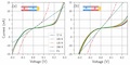
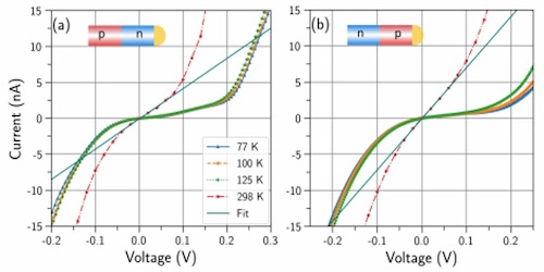
We have confirmed the presence of narrow, degenerately-doped axial silicon nanowire (SiNW) p-n junctions via off-axis electron holography (EH). SiNWs were grown via the vapor-solid-liquid (VLS) mechanism using gold (Au) as the catalyst, silane (SiH4), diborane (B2H6) and phosphine (PH3) as the precursors, and hydrochloric acid (HCl) to stabilize the growth. Two types of growth were carried out, and in each case we explored growth with both n/p and p/n sequences. In the first type, we abruptly switched the dopant precursors at the desired junction location, and in the second type we slowed the growth rate at the junction to allow the dopants to readily leave the Au catalyst. We demonstrate degenerately-doped p/n and n/p nanowire segments with abrupt potential profiles of 1.02±0.02 and 0.86±0.3 V, and depletion region widths as narrow as 10±1 nm via EH. Low temperature current-voltage measurements show an asymmetric curvature in the forward direction that resemble planar gold-doped tunnel junctions, where the tunneling current is hidden by a large excess current. The results presented herein show that the direct VLS growth of degenerately-doped axial SiNW p-n junctions is feasible, an essential step in the fabrication of more complex SiNW-based devices for electronics and solar energy.
Science
Ratcheting effects play an important role in systems ranging from mechanical socket wrenches to biological motor proteins. The underlying principle is to convert a fluctuating, unbiased force into unidirectional motion. Here, we report the ratcheting of electrons at room temperature using a semiconductor nanowire with precisely engineered asymmetry. Modulation of the nanowire diameter creates a cylindrical sawtooth geometry with broken inversion symmetry on a nanometer-length scale. In a two-terminal device, this structure responded as a three-dimensional geometric diode that funnels electrons preferentially in one direction through specular reflection of quasi-ballistic electrons at the nanowire surface. The ratcheting effect causes charge rectification at frequencies exceeding 40 gigahertz, demonstrating the potential for applications such as high-speed data processing and long-wavelength energy harvesting.
ACS Nano
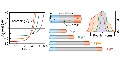
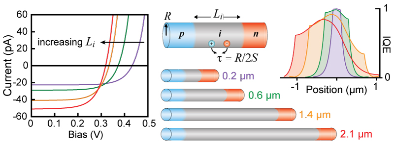
Nanowires (NWs) with axial p-i-n junctions have been widely explored as microscopic diodes for optoelectronic and solar energy applications, and their performance is strongly influenced by charge recombination at the surface. We delineate how the photovoltaic performance of these diodes is dictated not simply by the surface, however, but also by the complex and seemingly counterintuitive interplay of diode geometry—i.e. radius (R) and intrinsic length (Li)—with the surface recombination velocity (S). An analytical model to describe these relationships is developed and compared to finite-element simulations, which verify the accuracy and limitations of the model. The dependence of the dark saturation current (Io), internal quantum efficiency (IQE), short-circuit current (ISC), and open-circuit voltage (VOC) on both geometric and recombination parameters demonstrates that no single set of parameters produces optimal performance; instead, various tradeoffs in performance are observed. For instance, longer Li might be expected to produce higher ISC, yet at high values of S the ISC declines because of decreases in IQE. Moreover, longer Li produces a concurrent decline in VOC regardless of S due to increases in Io. We also find that ISC and VOC trends are radius-independent, yet Io is directly proportional to R, causing NWs with smaller R to display higher turn-on voltages. The analysis regarding the interplay of these parameters, verified by experimental measurements with various p-i-n geometries and surface treatments, provides clear guidance for the rational design of performance metrics for photodiode and photovoltaic devices.
ACS Applied Materials and Interfaces
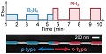
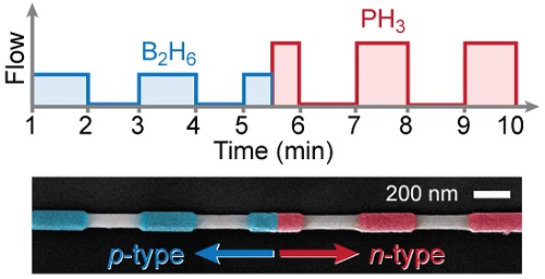
Although silicon (Si) nanowires (NWs) grown by a vapor–liquid–solid (VLS) mechanism have been demonstrated for a range of photonic, electronic, and solar-energy applications, continued progress with these NW-based technologies requires increasingly precise compositional and morphological control of the growth process. However, VLS growth typically encounters problems such as nonselective deposition on sidewalls, inadvertent kinking, unintentional or inhomogeneous doping, and catalyst-induced compositional gradients. Here, we overcome several of these difficulties and report the synthesis of uniform, linear, and degenerately doped Si NW superlattices with abrupt transitions between p-type, intrinsic, and n-type segments. The synthesis of these structures is enabled by in situ chlorination of the NW surface with hydrochloric acid (HCl) at temperatures ranging from 500 to 700 °C, yielding uniform NWs with minimal nonselective growth. Surprisingly, we find the boron (B) doping level in p-type segments to be at least 1 order of magnitude above the solid solubility limit, an effect that we attribute to a high incorporation of B in the liquid catalyst and kinetic trapping of B during crystallization at the liquid–solid interface to yield a highly nonequilibrium concentration. For growth at 510 °C, four-point-probe measurements yield active doping levels of at least 4.5 × 10^19 cm–3, which is comparable to the phosphorus (P) doping level of n-type segments. Because the B and P dopants are in sufficiently high concentrations for the Si to be degenerately doped, both segments inhibit the etching of Si in aqueous potassium hydroxide (KOH) solution. Moreover, we find that the dopant transitions are abrupt, facilitating nanoscale morphological control in both B- and P-doped segments through selective KOH etching of the NW with a spatial resolution of ∼10 nm. The results presented herein enable the growth of complex, degenerately doped p–n junction nanostructures that can be explored for a variety of advanced applications, such as Esaki diodes, multijunction solar cells, and tunneling field-effect transistors.