
Dr. Joe ChristesenThe Univ. of North Carolina, Ph.D. Chemistry, 2016 The College of William and Mary, B.S. Chemistry & Computer Science, 2011 |

|
First Author
ACS Journal of Physical Chemistry Letters
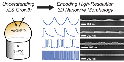
The patterning of semiconductors with nanometer-scale precision is a cornerstone of modern technology. Top-down methods, ranging from photolithography to focused-ion beam milling, are typically used to fabricate complex nanostructures. In this Perspective, we discuss an alternative bottom-up method to encode similar high-resolution morphology in semiconductor nanowires (NWs). This process, termed ENGRAVE for “Encoded Nanowire GRowth and Appearance through VLS and Etching”, combines fast modulation of nanowire composition during vapor–liquid–solid (VLS) growth with composition-dependent wet-chemical etching. This method produces cylindrically symmetric structures in which the diameter is modulated on a sub-10 nm axial length scale. The process can produce patterns that range from periodic, centrosymmetric to nonperiodic, asymmetric structures, including gratings, fractals, tapers, ratchets, sinusoids, nanogaps, and nanodots. We discuss the prospect for the ENGRAVE process to become a complementary method of lithographic-like patterning that encodes unique morphologies and physical properties in semiconductors for a range of technologies.
Semiconductor nanowires (NWs) are often synthesized by the vapor-liquid-solid (VLS) mechanism, a process in which a liquid droplet—supplied with precursors in the vapor phase—catalyzes the growth of a solid, crystalline NW. By changing the supply of precursors, the NW composition can be altered as it grows to create axial heterostructures, which are applicable to a range of technologies. The abruptness of the heterojunction is mediated by the liquid catalyst, which can act as a reservoir of material and impose a lower limit on the junction width. Here, we demonstrate that this “reservoir effect” is not a fundamental limitation and can be suppressed by selection of specific VLS reaction conditions. For Au-catalyzed Si NWs doped with P, we evaluate dopant profiles under a variety of synthetic conditions using a combination of elemental imaging with energy-dispersive x-ray spectroscopy and dopant-dependent wet-chemical etching. We observe a diameter-dependent reservoir effect under most conditions. However, at sufficiently slow NW growth rates (≤ 250 nm/min) and low reactor pressures (≤ 40 Torr), the dopant profiles are diameter independent and radially uniform with abrupt, sub-10 nm axial transitions. A kinetic model of NW doping, including the microscopic processes of (1) P incorporation into the liquid catalyst, (2) P evaporation from the catalyst, and (3) P crystallization in the Si NW, quantitatively explains the results and shows that suppression of the reservoir effect can be achieved when P evaporation is much faster than P crystallization. We expect similar reaction conditions can be developed for other NW systems and will facilitate the development of NW-based technologies that require uniform and abrupt heterostructures.
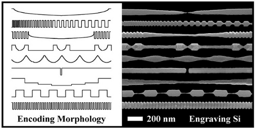
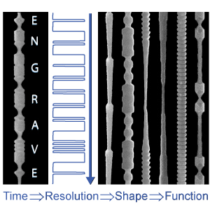
Si nanowires (NWs) have been widely explored as a platform for photonic and electronic technologies. Here, we report a bottom-up method to break the conventional “wire” symmetry and synthetically encode a high-resolution array of arbitrary shapes, including nanorods, sinusoids, bowties, tapers, nanogaps, and gratings, along the NW growth axis. Rapid modulation of phosphorus doping combined with selective wet-chemical etching enabled morphological features as small as 10 nm to be patterned over wires more than 50 μm in length. This capability fundamentally expands the set of technologies that can be realized with Si NWs, and as proof-of-concept, we demonstrate two distinct applications. First, nanogap-encoded NWs were used as templates for Noble metals, yielding plasmonic structures with tunable resonances for surface-enhanced Raman imaging. Second, core/shell Si/SiO2 nanorods were integrated into electronic devices that exhibit resistive switching, enabling nonvolatile memory storage. Moving beyond these initial examples, we envision this method will become a generic route to encode new functionality in semiconductor NWs.
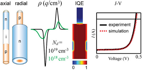
Semiconductor nanowires (NWs) are a developing platform for electronic and photonic technologies, and many demonstrated devices utilize a p-type/n-type (p–n) junction encoded along either the axial or radial directions of the wires. These miniaturized junctions enable a diverse range of functions, from sensors to solar cells, yet the physics of the devices has not been thoroughly evaluated. Here, we present finite-element modeling of axial and radial Si NW p–n junctions with total diameters of 240 nm and donor/acceptor doping levels ranging from 1016 to 1020 cm–3. We evaluate the photovoltaic performance of horizontally oriented NWs under 1 sun illumination and compare simulated current–voltage data to experimental measurements, permitting detailed analysis of NW performance, limitations, and prospect as a technology for solar energy conversion. Although high surface-to-volume ratios are cited as detrimental to NW performance, radial p–n junctions are surprisingly insensitive to surface recombination, with devices supporting open-circuit voltages (VOC) of 0.54 V and internal quantum efficiencies of 95% even with high surface recombination velocities (SRVs) of 105 cm/s. Axial devices, in which the depletion region is exposed to the surface, are far more sensitive to SRV, requiring substantially lower values of 103–104 cm/s to produce the same level of performance. For low values of the SRV (<100 cm/s), both axial and radial NWs can support VOC values of >0.70 V if the bulk minority carrier lifetime is 1 μs or greater. Experimental measurements on NWs grown by a vapor–liquid–solid mechanism yield VOC of 0.23 and 0.44 V for axial and radial NWs, respectively, and show that axial devices are limited by a SRV of 7 × 103 cm/s while radial devices are limited by a bulk lifetime of 3 ns. The simulations show that with further development the electrical characteristics of 200–300 nm Si NWs are sufficient to support power-conversion efficiencies of 15–25%. The analysis presented here can be generalized to other semiconductor homo- and heterojunctions, and we expect that insights from finite element modeling will serve as a powerful method to guide the design of advanced nanoscale structures.
Contributing Author


Science
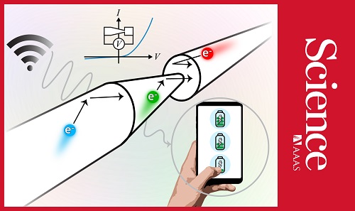
Ratcheting effects play an important role in systems ranging from mechanical socket wrenches to biological motor proteins. The underlying principle is to convert a fluctuating, unbiased force into unidirectional motion. Here, we report the ratcheting of electrons at room temperature using a semiconductor nanowire with precisely engineered asymmetry. Modulation of the nanowire diameter creates a cylindrical sawtooth geometry with broken inversion symmetry on a nanometer-length scale. In a two-terminal device, this structure responded as a three-dimensional geometric diode that funnels electrons preferentially in one direction through specular reflection of quasi-ballistic electrons at the nanowire surface. The ratcheting effect causes charge rectification at frequencies exceeding 40 gigahertz, demonstrating the potential for applications such as high-speed data processing and long-wavelength energy harvesting.
ACS Applied Materials and Interfaces
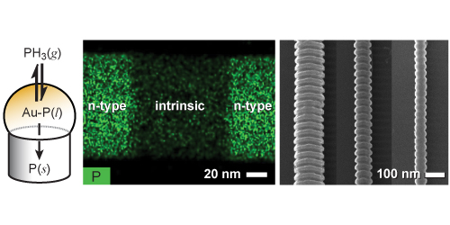
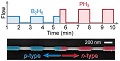
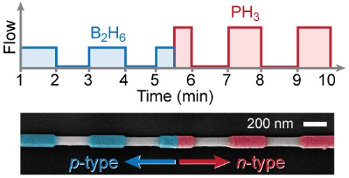
Although silicon (Si) nanowires (NWs) grown by a vapor–liquid–solid (VLS) mechanism have been demonstrated for a range of photonic, electronic, and solar-energy applications, continued progress with these NW-based technologies requires increasingly precise compositional and morphological control of the growth process. However, VLS growth typically encounters problems such as nonselective deposition on sidewalls, inadvertent kinking, unintentional or inhomogeneous doping, and catalyst-induced compositional gradients. Here, we overcome several of these difficulties and report the synthesis of uniform, linear, and degenerately doped Si NW superlattices with abrupt transitions between p-type, intrinsic, and n-type segments. The synthesis of these structures is enabled by in situ chlorination of the NW surface with hydrochloric acid (HCl) at temperatures ranging from 500 to 700 °C, yielding uniform NWs with minimal nonselective growth. Surprisingly, we find the boron (B) doping level in p-type segments to be at least 1 order of magnitude above the solid solubility limit, an effect that we attribute to a high incorporation of B in the liquid catalyst and kinetic trapping of B during crystallization at the liquid–solid interface to yield a highly nonequilibrium concentration. For growth at 510 °C, four-point-probe measurements yield active doping levels of at least 4.5 × 10^19 cm–3, which is comparable to the phosphorus (P) doping level of n-type segments. Because the B and P dopants are in sufficiently high concentrations for the Si to be degenerately doped, both segments inhibit the etching of Si in aqueous potassium hydroxide (KOH) solution. Moreover, we find that the dopant transitions are abrupt, facilitating nanoscale morphological control in both B- and P-doped segments through selective KOH etching of the NW with a spatial resolution of ∼10 nm. The results presented herein enable the growth of complex, degenerately doped p–n junction nanostructures that can be explored for a variety of advanced applications, such as Esaki diodes, multijunction solar cells, and tunneling field-effect transistors.
ACS Nano
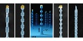
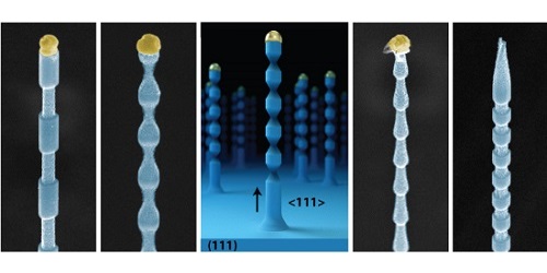
Vertically aligned semiconductor nanowires (NWs) have many potential applications for NW-based technologies, ranging from solar cells to intracellular sensors. Aligned NWs can be fabricated by top-down etching of planar wafers or synthesized from the bottom up using the vapor–liquid–solid (VLS) mechanism to induce epitaxial growth on lattice-matched substrates. The VLS process permits the modulation of dopants along the NW growth axis, which if combined with dopant-dependent wet-chemical etching, can be used to encode precise morphology. However, the synthesis of vertical and linear NWs with complex morphology is nontrivial, requiring control over multiple interdependent aspects of the VLS process. Here, we demonstrate sub-10 nm morphology in ⟨111⟩ epitaxial silicon (Si) NWs grown by the VLS mechanism on (111) Si substrates with gold (Au) catalysts. Using silane (SiH4), phosphine (PH3), and hydrochloric acid (HCl) precursor gases at 480 °C, precise morphology is encoded through abrupt phosphorus (P) dopant transitions, which are found to be less than 5 nm in width. The results highlight three mechanistic attributes of the process. First, NW growth in the ⟨111⟩ direction is found to be unstable at high SiH4 partial pressures and growth rates unless using HCl, which stabilizes NW growth through chlorination of the NW sidewall. Second, aggregated Au deposited on the NW surface by the VLS catalyst is found to be immobile on the chlorinated surface and to impede selective wet-chemical etching by potassium hydroxide (KOH) solution, preventing the design of precise morphology. Third, the aggregation of Au is found to be strongly dependent on the SiH4 partial pressure and NW growth rate, and values exceeding ∼100 mTorr and ∼150 nm/min, respectively, are required to minimize Au and thereby enable selective wet-chemical etching. Under optimized growth conditions, we find that abrupt, complex, and arbitrary dopant profiles and morphologies can be encoded in vertical Si NWs, and we expect that a variety of electronic and photonic applications can be realized with these designed nanostructures.
ACS Journal of Physical Chemistry Letters
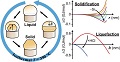
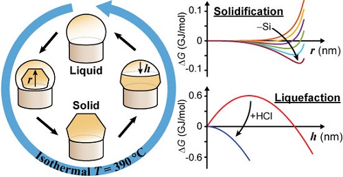
Knowledge of nucleation and growth mechanisms is essential for the synthesis of nanomaterials, such as semiconductor nanowires, with shapes and compositions precisely engineered for technological applications. Nanowires are conventionally grown by the seemingly well-understood vapor–liquid–solid mechanism, which uses a liquid alloy as the catalyst for growth. However, we show that it is possible to instantaneously and reversibly switch the phase of the catalyst between a liquid and superheated solid state under isothermal conditions above the eutectic temperature. The solid catalyst induces a vapor–solid–solid growth mechanism, which provides atomic-level control of dopant atoms in the nanowire. The switching effect cannot be predicted from equilibrium phase diagrams but can be explained by the dominant role of the catalyst surface in modulating the kinetics and thermodynamics of phase behavior. The effect should be general to metal-catalyzed nanowire growth and highlights the unexpected yet technologically relevant nonequilibrium effects that can emerge in the growth of nanoscale systems.
Nano Letters
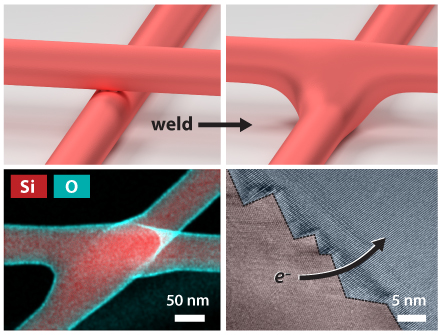
Semiconductor nanowires (NWs) have been demonstrated as a potential platform for a wide-range of technologies, yet a method to interconnect functionally encoded NWs has remained a challenge. Here, we report a simple capillarity-driven and self-limited welding process that forms mechanically robust and Ohmic inter-NW connections. The process occurs at the point-of-contact between two NWs at temperatures 400–600 °C below the bulk melting point of the semiconductor. It can be explained by capillarity-driven surface diffusion, inducing a localized geometrical rearrangement that reduces spatial curvature. The resulting weld comprises two fused NWs separated by a single, Ohmic grain boundary. We expect the welding mechanism to be generic for all types of NWs and to enable the development of complex interconnected networks for neuromorphic computation, battery and solar cell electrodes, and bioelectronic scaffolds.
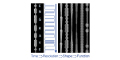
Bottom-up, chemical methods to control the morphology of semiconductor nanostructures are a promising complement to the top-down fabrication techniques that currently dominate the semiconductor industry. Among bottom-up techniques, nanowire (NW) growth using the vapor–liquid–solid (VLS) mechanism has received great attention. In this Highlight article, we review our recent progress toward understanding the microscopic processes that govern VLS NW growth, doping, and dopant modulation. Quantitative measurements of Si NW growth rates and P dopant profiles under a range of synthetic conditions are interpreted with a kinetic analysis of VLS growth that includes the microscopic reactions of incorporation, evaporation, and crystallization. The analysis allows us to identify synthetic conditions that yield both diameter-independent growth rates and abrupt, diameter-independent dopant transitions. The optimized conditions allow precise, sub-10 nm morphology to be encoded along the growth axis of Si NWs, enabling the bottom-up chemical nanofabrication of complex structures that are typically fabricated by high-resolution, top-down lithography.
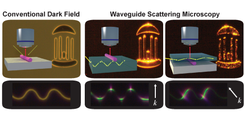
Dark-field microscopy (DFM) is widely used to optically image and spectroscopically analyze nanoscale objects. In a typical DFM configuration, a sample is illuminated at oblique angles and an objective lens collects light scattered by the sample at a range of lower angles. Here, we develop waveguide scattering microscopy (WSM) as an alternative technique to image and analyze photonic nanostructures. WSM uses an incoherent white-light source coupled to a dielectric slab waveguide to generate an evanescent field that illuminates objects located within several hundred nanometers of the waveguide surface. Using standard microscope slides or coverslips as the waveguide, we demonstrate high-contrast dark-field imaging of nanophotonic and plasmonic structures such as Si nanowires, Au nanorods, and Ag nanoholes. Scattering spectra collected in the WSM configuration show excellent signal-to-noise with minimal background signal compared to conventional DFM. In addition, the polarization of the incident field is controlled by the direction of the propagating wave, providing a straightforward route to excite specific optical modes in anisotropic nanostructures by selecting the appropriate input wavevector. Considering the facile integration of WSM with standard microscopy equipment, we anticipate it will become a versatile tool for characterizing photonic nanostructures.
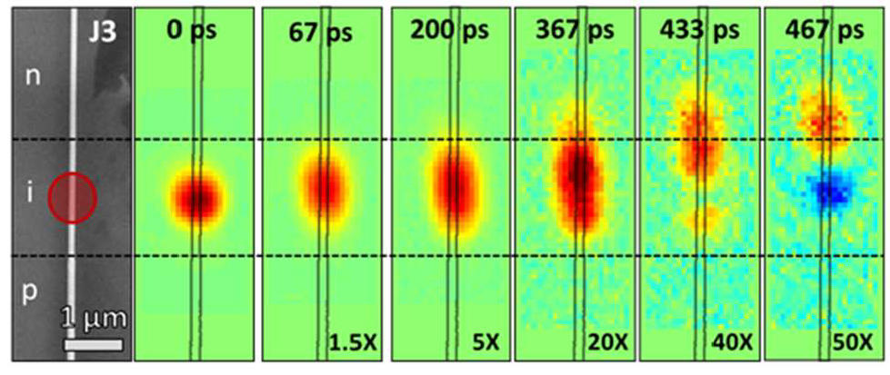
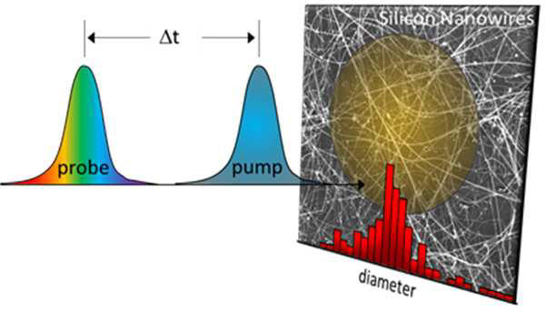
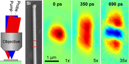
Silicon nanowires incorporating p-type/n-type (p-n) junctions have been introduced as basic building blocks for future nanoscale electronic components. Controlling charge flow through these doped nanostructures is central to their function, yet our understanding of this process is inferred from measurements that average over entire structures or integrate over long times. Here, we have used femtosecond pump–probe microscopy to directly image the dynamics of photogenerated charge carriers in silicon nanowires encoded with p-n junctions along the growth axis. Initially, motion is dictated by carrier–carrier interactions, resulting in diffusive spreading of the neutral electron–hole cloud. Charge separation occurs at longer times as the carrier distribution reaches the edges of the depletion region, leading to a persistent electron population in the n-type region. Time-resolved visualization of the carrier dynamics yields clear, direct information on fundamental drift, diffusion, and recombination processes in these systems, providing a powerful tool for understanding and improving materials for nanotechnology.
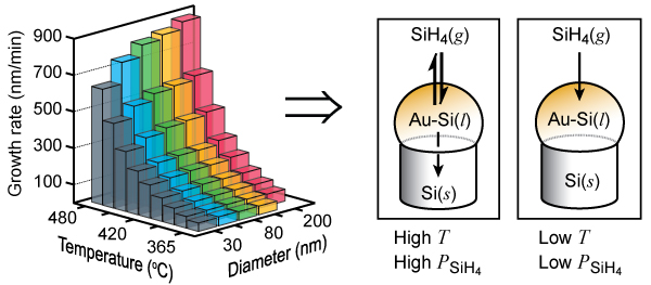
The vapor–liquid–solid (VLS) mechanism is widely used for the synthesis of semiconductor nanowires (NWs), yet several aspects of the mechanism are not fully understood. Here, we present comprehensive experimental measurements on the growth rate of Au-catalyzed Si NWs over a range of temperatures (365–480 °C), diameters (30–200 nm), and pressures (0.1–1.6 Torr SiH4). We develop a kinetic model of VLS growth that includes (1) Si incorporation into the liquid Au–Si catalyst, (2) Si evaporation from the catalyst surface, and (3) Si crystallization at the catalyst–NW interface. This simple model quantitatively explains growth rate data collected over more than 65 distinct synthetic conditions. Surprisingly, upon increasing the temperature and/or pressure, the analysis reveals an abrupt transition from a diameter-independent growth rate that is limited by incorporation to a diameter-dependent growth rate that is limited by crystallization. The identification of two distinct growth regimes provides insight into the synthetic conditions needed for specific NW-based technologies, and our kinetic model provides a straightforward framework for understanding VLS growth with a range of metal catalysts and semiconductor materials.
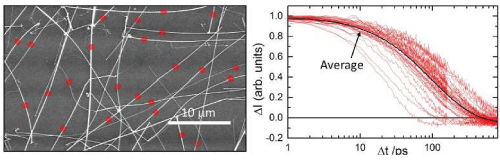
Ultrafast charge carrier dynamics in silicon nanowires (NWs) grown by a vapor–liquid–solid mechanism were interrogated with optical pump–probe microscopy. The high time and spatial resolutions achieved by the experiments provide insight into the charge carrier dynamics of single nanostructures. Individual NWs were excited by a femtosecond pump pulse focused to a diffraction-limited spot, producing photogenerated carriers (electrons and holes) in a localized region of the structure. Photoexcited carriers undergo both electron–hole recombination and diffusional migration away from the excitation spot on similar time scales. The evolution of the carrier population is monitored by a delayed probe pulse that is also focused to a diffraction-limited spot. When the pump and probe are spatially overlapped, the transient signal reflects both recombination and carrier migration. Diffusional motion is directly observed by spatially separating the pump and probe beams, enabling carriers to be generated in one location and detected in another. Quantitative analysis of the signals yields a statistical distribution of carrier lifetimes from a large number of individual NWs. On average, the lifetime was found to be linearly proportional to the diameter, consistent with a surface-mediated recombination mechanism. These results highlight the capability of pump–probe microscopy to quantitatively evaluate key recombination characteristics in semiconductor nanostructures, which are important for their implementation in nanotechnologies.
Ultrafast carrier dynamics in silicon nanowires with average diameters of 40, 50, 60, and 100 nm were studied with transient absorption spectroscopy. After 388 nm photoexcitation near the direct band gap of silicon, broadband spectra from 400 to 800 nm were collected between 200 fs and 1.3 ns. The transient spectra exhibited both absorptive and bleach features that evolved on multiple time scales, reflecting contributions from carrier thermalization and recombination as well as transient shifts of the ground-state absorption spectrum. The initially formed “hot” carriers relaxed to the band edge within the first ∼300 fs, followed by recombination over several hundreds of picoseconds. The charge carrier lifetime progressively decreased with decreasing diameter, a result consistent with a surface-mediated recombination process. Recombination dynamics were quantitatively modeled using the diameter distribution measured from each sample, and this analysis yielded a consistent surface recombination velocity of ∼2 × 104 cm/s across all samples. The results indicate that transient absorption spectroscopy, which interrogates thousands of individual nanostructures simultaneously, can be an accurate probe of material parameters in inhomogeneous semiconductor samples when geometrical differences within the ensemble are properly analyzed.
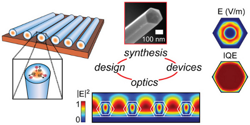
The silicon p–n junction is the most successful solar energy technology to date, yet it accounts for a marginal percentage of worldwide energy production. To change the status quo, a disruptive technological breakthrough is needed. In this Perspective, we discuss the potential for complex silicon nanowires to serve as a platform for next-generation photovoltaic devices. We review the synthesis, electrical characteristics, and optical properties of core/shell silicon nanowires that are subwavelength in diameter and contain radial p–n junctions. We highlight the unique features of these nanowires, such as optical antenna effects that concentrate light and intense built-in electric fields that enable ultrafast charge-carrier separation. We advocate a paradigm in which nanowires are arranged in periodic horizontal arrays to form ultrathin devices. Unlike conventional planar silicon, nanowire structures provide the flexibility to incorporate multiple semiconductor, dielectric, and metallic materials in a single system, providing the foundation for a disruptive, unconventional solar energy technology.
We have developed a pump–probe microscope capable of exciting a single semiconductor nanostructure in one location and probing it in another with both high spatial and temporal resolution. Experiments performed on Si nanowires enable a direct visualization of the charge cloud produced by photoexcitation at a localized spot as it spreads along the nanowire axis. The time-resolved images show clear evidence of rapid diffusional spreading and recombination of the free carriers, which is consistent with ambipolar diffusion and a surface recombination velocity of ∼104 cm/s. The free carrier dynamics are followed by trap carrier migration on slower time scales.